Whenever the Am79C978 controller is the current bus
master and a data parity error occurs, SINT (CSR5, bit
11) will be set to 1. When SINT is set, INTA is asserted
if the enable bit SINTE (CSR5, bit 10) is set to 1. This
mechanism can be used to inform the driver of the sys-
tem error. The host can read the PCI Status register to
determine the exact cause of the interrupt. The setting
of SINT due to a data parity error is not dependent on
the setting of PERREN (PCI Command register, bit 6).
will be terminated immediately, generating a runt
packet.
If 512 bits or more have been transmitted, the message
will have the current FCS inverted and appended at the
next byte boundary to guarantee an FCS error is de-
tected at the receiving station.
APERREN does not affect the reporting of address
parity errors or data parity errors that occur when the
Am79C978 controller is the target of the transfer.
By default, a data parity error does not affect the state
of the MAC engine. TheAm79C978 controller treats the
data in all bus master transfers that have a parity error
as if nothing has happened. All network activity contin-
ues.
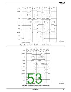
Initialization Block DMA Transfers
During execution of the Am79C978 controller bus mas-
ter initialization procedure, the microcode will repeat-
edly request DMA transfers from the BIU. During each
of these initialization block DMA transfers, the BIU will
perform two data transfer cycles reading one DWord
per transfer and then it will relinquish the bus. When
SSIZE32 (BCR20, bit 8) is set to 1 (i.e., the initialization
block is organized as 32-bit software structures), there
are seven DWords to transfer during the bus master ini-
tialization procedure, so four bus mastership periods
are needed in order to complete the initialization se-
quence. Note that the last DWord transfer of the last
bus mastership period of the initialization sequence ac-
cesses an unneeded location. Data from this transfer is
discarded internally. When SSIZE32 is cleared to 0
(i.e., the initialization block is organized as 16-bit soft-
ware structures), then three bus mastership periods
are needed to complete the initialization sequence.
Advanced Parity Error Handling
For all DMA cycles, the Am79C978 controller provides
a second, more advanced level of parity error handling.
This mode is enabled by setting APERREN (BCR20, bit
10) to 1. When APERREN is set to 1, the BPE bits
(RMD1 and TMD1, bit 23) are used to indicate parity
error in data transfers to the receive and transmit buff-
ers. Note that since the advanced parity error handling
uses an additional bit in the descriptor, SWSTYLE
(BCR20, bits 7-0) must be set to 2 or 3 to program the
Am79C978 controller to use 32-bit software structures.
TheAm79C978 controller will react in the following way
when a data parity error occurs:
n Initialization block read: STOP (CSR0, bit 2) is set
to 1 and causes a STOP_RESET of the device.
The Am79C978 device supports two transfer modes
for reading the initialization block: non-burst and burst
mode, with burst mode being the preferred mode when
the Am79C978 controller is used in a PCI bus applica-
tion. See Figure 25 and Figure 26.
n Descriptor ring read: Any on-going networkactivity
is terminated in an orderly sequence and then STOP
(CSR0, bit 2) is set to 1 to cause a STOP_RESET
of the device.
n Descriptor ring write: Any on-going network activity
is terminated in an orderly sequence and then STOP
(CSR0, bit 2) is set to 1 to cause a STOP_RESET
of the device.
When BREADE is cleared to 0 (BCR18, bit 6), all initial-
ization block read transfers will be executed in non-
burst mode. There is a new address phase for every
data phase. FRAME will be dropped between the two
transfers. The two phases within a bus mastership pe-
riod will have addresses of ascending contiguous or-
der.
n Transmit buffer read: BPE (TMD1, bit 23) is set in
the current transmit descriptor. Any on-going net-
work transmission is terminated in an orderly se-
quence.
When BREADE is set to 1 (BCR18, bit 6), all initializa-
tion block read transfers will be executed in burst
mode. AD[1:0] will be 0 during the address phase indi-
cating a linear burst order.
n Receive buffer write: BPE (RMD1, bit 23) is set in
the last receive descriptor associated with the frame.
Terminating on-going network transmission in an or-
derly sequence means that if less than 512 bits have
been transmitted onto the network, the transmission
52
Am79C978

 AMD [ AMD ]