D A T A S H E E T
other system tasks. In this case, the system must start
mand. When the time-out period is complete, DQ3
switches from a “0” to a “1.” If the time between addi-
tional sector erase commands from the system can be
assumed to be less than 50 µs, the system need not
monitor DQ3. See also the Sector Erase Command
Sequence section.
at the beginning of the algorithm when it returns to de-
termine the status of the operation (top of Figure 9).
DQ5: Exceeded Timing Limits
DQ5 indicates whether the program, erase, or
write-to-buffer time has exceeded a specified internal
pulse count limit. Under these conditions DQ5 produces a
“1,” indicating that the program or erase cycle was not suc-
cessfully completed.
After the sector erase command is written, the system
should read the status of DQ7 (Data# Polling) or DQ6
(Toggle Bit I) to ensure that the device has accepted
the command sequence, and then read DQ3. If DQ3 is
“1,” the Embedded Erase algorithm has begun; all fur-
ther commands (except Erase Suspend) are ignored
until the erase operation is complete. If DQ3 is “0,” the
device will accept additional sector erase commands.
To ensure the command has been accepted, the sys-
tem software should check the status of DQ3 prior to
and following each subsequent sector erase com-
mand. If DQ3 is high on the second status check, the
last command might not have been accepted.
The device may output a “1” on DQ5 if the system tries
to program a “1” to a location that was previously pro-
grammed to “0.” Only an erase operation can
change a “0” back to a “1.” Under this condition, the
device halts the operation, and when the timing limit
has been exceeded, DQ5 produces a “1.”
In all these cases, the system must write the reset
command to return the device to the reading the array
(or to erase-suspend-read if the device was previously
in the erase-suspend-program mode).
Table 14 shows the status of DQ3 relative to the other
status bits.
DQ3: Sector Erase Timer
DQ1: Write-to-Buffer Abort
After writing a sector erase command sequence, the
system may read DQ3 to determine whether or not
erasure has begun. (The sector erase timer does not
apply to the chip erase command.) If additional
sectors are selected for erasure, the entire time-out
also applies after each additional sector erase com-
DQ1 indicates whether a Write-to-Buffer operation
was aborted. Under these conditions DQ1 produces a
“1”.
The
system
must
issue
the
Write-to-Buffer-Abort-Reset command sequence to re-
turn the device to reading array data. See Write Buffer
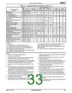
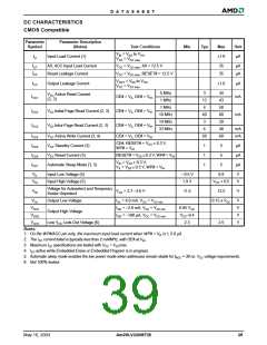
Table 14. Write Operation Status
DQ7
DQ5
DQ2
Status
(Note 2)
DQ6
(Note 1)
DQ3
N/A
1
(Note 2)
DQ1 RY/BY#
Embedded Program Algorithm
Embedded Erase Algorithm
Program-Suspended
DQ7#
0
Toggle
Toggle
0
0
No toggle
Toggle
0
0
0
Standard
Mode
N/A
Invalid (not allowed)
Data
1
1
1
1
0
Program
Suspend
Mode
Program-
Sector
Suspend
Non-Program
Read
Suspended Sector
Erase-Suspended
1
No toggle
Toggle
0
N/A
Toggle
N/A
N/A
N/A
Erase-
Sector
Suspend
Erase
Suspend
Mode
Non-EraseSuspended
Read
Data
Sector
Erase-Suspend-Program
(Embedded Program)
DQ7#
0
N/A
Busy (Note 3)
Abort (Note 4)
DQ7#
DQ7#
Toggle
Toggle
0
0
N/A
N/A
N/A
N/A
0
1
0
0
Write-to-
Buffer
Notes:
1. DQ5 switches to ‘1’ when an Embedded Program, Embedded Erase, or Write-to-Buffer operation has exceeded the
maximum timing limits. Refer to the section on DQ5 for more information.
2. DQ7 and DQ2 require a valid address when reading status information. Refer to the appropriate subsection for further details.
3. The Data# Polling algorithm should be used to monitor the last loaded write-buffer address location.
4. DQ1 switches to ‘1’ when the device has aborted the write-to-buffer operation.
May 16, 2003
Am29LV320MT/B
37

 AMD [ AMD ]