D A T A S H E E T
REVISION SUMMARY
Distinctive Characteristics
Revision A (May 1997)
Added:
Initial release of Am29F016B (0.35 µm) device.
■ 20-year data retention at 125°C
— Reliable operation for the life of the system
DC Characteristics—CMOS Compatible
Revision B (January 1998)
Global
Made formatting and layout consistent with other data
sheets. Used updated common tables and diagrams.
I
, I
: Added Note 4, “For CMOS mode only I
,
CC3 CC4
CC3
I
= 20 µA at extended temperature (>+85°C)”.
CC4
Revision B+1 (January 1998)
AC Characteristics—Read-only Operations
DC Characteristics—TTL/NMOS Compatible and
CMOS Compatible
Deleted note referring to output driver disable time.
I
, I
, I
, I
: Added Note 2 “Maximum I
CC1 CC2 CC3 CC4 CC
specifications are tested with V = V
”.
CCmax
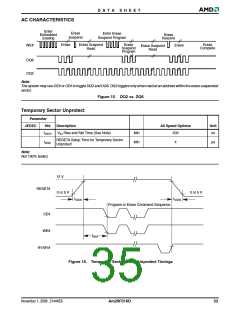
Figure 16—Temporary Sector Group Unprotect
Timings
CC
I
, I
: Deleted V = V Max.
CC3 CC4 CC CC
Corrected title to indicate “sector group.”
Revision C+1 (March 23, 1999)
Operating Ranges
Revision B+2 (April 1998)
Global
The temperature ranges are now specified as ambient.
Added -70 speed option, deleted -75 speed option.
Revision C+2 (May 17, 1999)
Product Selector Guide
Distinctive Characteristics
Changed minimum 100K write/erase cycles guaran-
teed to 1,000,000.
Corrected the t specification for the -150 speed op-
tion to 55 ns.
OE
Ordering Information
Operating Ranges
Added extended temperature availability to -90, -120,
and -150 speed options.
V
Supply Voltages: Added “V for 5% devices .
CC
CC
+4.75 V to +5.25 V”.
Operating Ranges
Revision C+3 (July 2, 1999)
Global
Added extended temperature range.
DC Characteristics, CMOS Compatible
Added references to availability of device in Known
Good Die (KGD) form.
Corrected the CE# and RESET# test conditions for
I
and I
to V
0.5 V.
CC3
CC4
CC
Revision D (November 16, 1999)
AC Characteristics
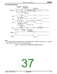
AC Characteristics—Figure 11. Program
Operations Timing and Figure 12. Chip/Sector
Erase Operations
Erase/Program Operations; Erase and Program Oper-
ations Alternate CE# Controlled Writes: Corrected the
notes reference for t
and t
. These param-
WHWH1
WHWH2
Deleted t
high.
and changed OE# waveform to start at
GHWL
eters are 100% tested. Corrected the note reference for
. This parameter is not 100% tested.
t
VCS
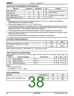
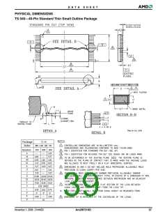
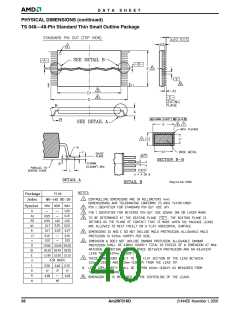
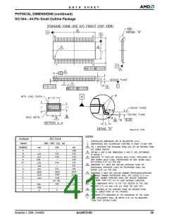
Physical Dimensions
Temporary Sector Unprotect Table
Replaced figures with more detailed illustrations.
Added note reference for t
100% tested.
. This parameter is not
VIDR
Revision E (May 19, 2000)
Global
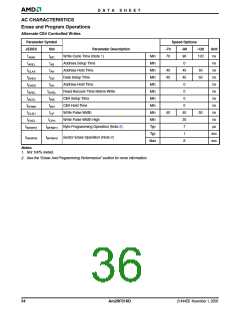
Erase and Programming Performance
Changed part number to Am29F016D. This reflects the
new 0.23 µm process technology upon which this de-
vice will now be built.
Changed minimum 100K program and erase cycles
guaranteed to 1,000,000.
Revision C (January 1999)
Global
The Am29F016D is compatible with the previous 0.32
µm Am29F016B device, with the exception of the sec-
tor group protect and unprotect algorithms. These
algorithms are provided in a seperate document. Con-
tact AMD for more information or to request a copy of
that document.
Updated for CS39S process technology.
40
Am29F016D
21444E6 November 2, 2006

 AMD [ AMD ]