D A T A S H E E T
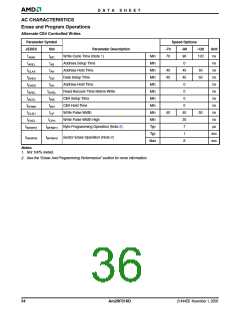
ERASE AND PROGRAMMING PERFORMANCE
Parameter
Sector Erase Time
Typ (Note 1)
Max (Note 2)
Unit
sec
sec
µs
Comments
1
32
7
8
Excludes 00h programming prior to
erasure (Note 4)
Chip Erase Time
256
300
43.2
Byte Programming Time
Chip Programming Time (Note 3)
Excludes system-level overhead
(Note 5)
14.4
sec
Notes:
1. Typical program and erase times assume the following conditions: 25°C, 5.0 V VCC, 1,000,000 cycles. Additionally,
programming typicals assume checkerboard pattern.
2. Under worst case conditions of 90°C, VCC = 4.5 V, 1,000,000 cycles.
3. The typical chip programming time is considerably less than the maximum chip programming time listed, since most bytes
program faster than the maximum byte program time listed. If the maximum byte program time given is exceeded, only then
does the device set DQ5 = 1. See the section on DQ5 for further information.
4. In the pre-programming step of the Embedded Erase algorithm, all bytes are programmed to 00h before erasure.
5. System-level overhead is the time required to execute the four-bus-cycle sequence for programming. See Table 6 for further
information on command definitions.
6. The device has a guaranteed minimum erase and program cycle endurance of 1,000,000 cycles.
LATCHUP CHARACTERISTICS
Min
Max
Input Voltage with respect to VSS on I/O pins
VCC Current
–1.0 V
VCC + 1.0 V
+100 mA
–100 mA
Note: Includes all pins except VCC. Test conditions: VCC = 5.0 Volt, one pin at a time.
TSOP AND SO PIN CAPACITANCE
Parameter
Symbol
Parameter Description
Input Capacitance
Test Conditions
Min
6
Max
7.5
12
Unit
CIN
VIN = 0
VOUT = 0
VIN = 0
pF
pF
pF
COUT
CIN2
Output Capacitance
8.5
7.5
Control Pin Capacitance
9
Notes:
1. Sampled, not 100% tested.
2. Test conditions TA = 25°C, f = 1.0 MHz.
DATA RETENTION
Parameter
Test Conditions
150°C
Min
10
Unit
Years
Years
Minimum Pattern Data Retention Time
125°C
20
36
Am29F016D
21444E6 November 1, 2006

 AMD [ AMD ]