P R E L I M I N A R Y
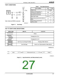
TEST CONDITIONS
Table 7. Test Specifications
Test Condition All
1 TTL gate
3.3 V
Unit
Output Load
2.7 kΩ
Device
Under
Test
Output Load Capacitance, C
(including jig capacitance)
L
100
pF
C
L
Input Rise and Fall Times
Input Pulse Levels
5
ns
6.2 kΩ
0.0–3.0
V
Input timing measurement reference
levels
1.5
1.5
V
V
Output timing measurement
reference levels
Note: Diodes are IN3064 or equivalent
21519A-15
Figure 11. Test Setup
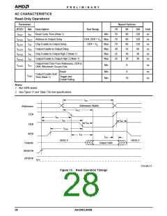
KEY TO SWITCHING WAVEFORMS
WAVEFORM
INPUTS
OUTPUTS
Steady
Changing from H to L
Changing from L to H
Don’t Care, Any Change Permitted
Does Not Apply
Changing, State Unknown
Center Line is High Impedance State (High Z)
KS000010-PAL
3.0 V
0.0 V
1.5 V
1.5 V
Input
Measurement Level
Output
21519A-16
Figure 12. Input Waveforms and Measurement Levels
Am29DL800B
27

 AMD [ AMD ]