P R E L I M I N A R Y
GENERAL DESCRIPTION
The Am29DL800B is an 8 Mbit, 3.0 volt-only flash
memory device, organized as 524,288 words or
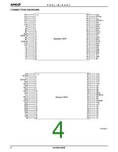
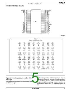
1,048,576 bytes. The device is offered in 44-pin SO,
48-pin TSOP, and 48-ball FBGA packages. The word-
wide (x16) data appears on DQ0–DQ15; the byte-wide
(x8) data appears on DQ0–DQ7. This device requires
only a single 3.0 volt VCC supply to perform read, pro-
gram, and erase operations. A standard EPROM pro-
grammer can also be used to program and erase the
device.
tates faster programming times by requiring only two
write cycles to program data instead of four.
Device erasure occurs by executing the erase com-
mand sequence. This initiates the Embedded Erase
algorithm—an internal algorithm that automatically
preprograms the array (if it is not already programmed)
before executing the erase operation. During erase, the
device automatically times the erase pulse widths and
verifies proper cell margin.
The host system can detect whether a program or
erase operation is complete by observing the RY/BY#
pin, or by reading the DQ7 (Data# Polling) and DQ6
(toggle) status bits. After a program or erase cycle has
been completed, the device automatically returns to
reading array data.
This device is manufactured using AMD’s 0.35 µm
process technology, and offers all the features and ben-
efits of the Am29DL800, which was manufactured
using a 0.5 µm technology.
The standard device offers access times of 70, 90, and
120 ns, allowing high-speed microprocessors to oper-
ate without wait states. Standard control pins—chip en-
able (CE#), write enable (WE#), and output enable
(OE#)—control read and write operations, and avoid
bus contention issues.
The sector erase architecture allows memory sectors
to be erased and reprogrammed without affecting the
data contents of other sectors. The device is fully
erased when shipped from the factory.
The device requires only a single 3.0 volt power sup-
ply for both read and write functions. Internally gener-
ated and regulated voltages are provided for the
program and erase operations.
Hardware data protection measures include a low
VCC detector that automatically inhibits write opera-
tions during power transitions. The hardware sector
protection feature disables both program and erase
operations in any combination of the sectors of mem-
ory. This can be achieved in-system or via program-
ming equipment.
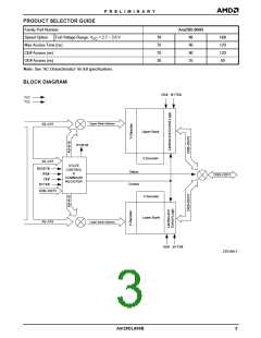
Simultaneous Read/Write Operations with
Zero Latency
The Simultaneous Read/Write architecture provides si-
multaneous operation by dividing the memory space
into two banks. Bank 1 contains eight boot/parameter
sectors, and Bank 2 consists of fourteen larger, code
sectors of uniform size. The device can improve overall
system performance by allowing a host system to pro-
gram or erase in one bank, then immediately and si-
multaneously read from the other bank, with zero
latency. This releases the system from waiting for the
completion of program or erase operations.
The Erase Suspend feature enables the user to put
erase on hold for any period of time to read data from,
or program data to, any sector within that bank that is
not selected for erasure. True background erase can
thus be achieved. There is no need to suspend the
erase operation if the read data is in the other bank.
The hardware RESET# pin terminates any operation
in progress and resets the internal state machine to
reading array data. The RESET# pin may be tied to the
system reset circuitry. A system reset would thus also
reset the device to reading array data, enabling the sys-
tem microprocessor to read the boot-up firmware from
the Flash memory.
Am29DL800B Features
The device offers complete compatibility with the
JEDEC single-power-supply Flash command set
standard. Commands are written to the command
register using standard microprocessor write timings.
Register contents serve as input to an internal state
machine that controls the erase and programming
circuitry. Write cycles also internally latch addresses
and data needed for the programming and erase
operations. Reading data out of the device is similar to
reading from other Flash or EPROM devices.
The device offers two power-saving features. When ad-
dresses have been stable for a specified amount of
time, the device enters the automatic sleep mode.
The system can also place the device into the standby
mode. Power consumption is greatly reduced in both
these modes.
AMD’s Flash technology combines years of Flash mem-
ory manufacturing experience to produce the highest
levels of quality, reliability, and cost effectiveness. The
device electrically erases all bits within a sector simulta-
neously via Fowler-Nordheim tunneling. The bytes are
programmed one byte or word at a time using hot elec-
tron injection.
Device programming occurs by executing the program
command sequence. This initiates the Embedded
Program algorithm—an internal algorithm that auto-
matically times the program pulse widths and verifies
proper cell margin. The Unlock Bypass mode facili-
2
Am29DL800B

 AMD [ AMD ]