Revision 1.02 – April 12, 2007
S5920 – PCI Product: Pass-Thru Operation
Data Book
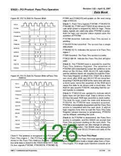
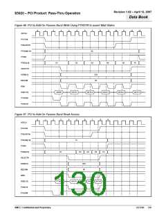
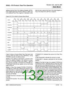
Figure 65. PCI to Add-On Passive Burst Write
3
4
7
8
9
0
1
2
5
6
10
11
12
13
ADCLK
PTATN#
PTBURST#
PTNUM[1:0]
PTWR
3h
PTBE[3:0]
SELECT#
ADR[6:2]
BE[3:0]#
RD#
D1
D2
D3
D4
Fh
2Ch
0h
0h
0h
0h
DQ[31:0]
PTADR#
PTRDY#
ADDR
DATA1 DATA2 DATA3 DATA4
Figure 7 shows a Passive mode PCI to Add-On burst
write of four DWORDs. In the following example, Add-
On logic incorporates the use of PTADR# followed by
multiple data reads to the S5920. If Add-On logic does
not support burst accesses, PTADR# can be pulsed
for individual data reads. The S5920 automatically
increments the address in the APTA register during
PCI bursts. In this example PTRDY# is continually
asserted, indicating that Add-On logic is capable of
accepting one DWORD per clock cycle. In addition,
the PTBE[3:0] signals indicate a unique byte-enable
for each data transfer.
PTWR and PTBE[3:0] will update on the next rising
edge of ADCLK.
Clock 1: Pass-Thru signals PTATN#, PTBURST#,
PTNUM[1:0], PTWR and PTBE[3:0] are driven to indi-
cate what action is required by Add-On logic. These
status signals are valid only when PTATN# is active.
Add-On logic can decode status signals upon the
assertion of PTATN#.
PTATN# Asserted. Indicates Pass-Thru access is
pending.
PTBURST# Asserted. The access has multiple data
phases.
The Pass-Thru Write FIFO (or APTD) can be disabled
for bursts (do not accept PCI posted writes). In this
case, the PCI is allowed to write to only one FIFO
location and cannot continue bursting until the add-on
has read the data. PTBURST# is never asserted when
the PCI write FIFO is disabled. For this example, the
Write FIFO is enabled.
PTNUM[1:0] 3h. Indicates the access is to Pass-Thru
region 3.
PTWR Asserted. Indicates the access is a write.
PTBE[3:0]# D1. Indicates valid bytes for the first data
transfer.
Clock 2: The PTADR# input is asserted to read the
Pass-Thru Address Register. The RD#, BE#, ADR[6:2]
and SELECT# inputs are driven during this clock to
read the Pass-Thru Data Register contents onto the
DQ bus during the next clock. PTRDY# is asserted,
indicating that the first transfer is complete.
Clock 0: The address is recognized as a PCI write to
Pass-Thru region 1. The PCI bus write address is
stored in the Pass-Thru Address Register. The PCI
bus write data is stored in the S5920 write FIFO. Add-
On bus signals PTATN#, PTBURST#, PTNUM[1:0],
AMCC Confidential and Proprietary
DS1596
128

 AMCC [ APPLIED MICRO CIRCUITS CORPORATION ]