Revision 1.02 – April 12, 2007
S5920 – PCI Product: Pass-Thru Operation
Data Book
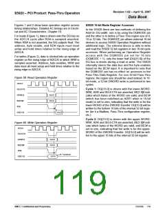
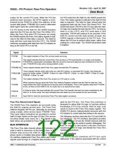
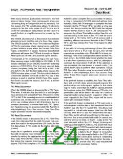
Figure 61. 16 Bit Mode Operation Register DWORD Write/Read
0
1234
56789
10
11
12
13
ADCLK
DQMODE
SELECT#
ADR[6:2]
BE3#
60h
10b
60h
00b
BE[1:0]#
WR#
00b
01b
RD#
DQ[15:0]
5678h
1234h
1234
5678h
Figure 3. 16 Bit Mode Operation Register DWORD
Write/Read Figure 3 shows an example of a DWORD
write of 12345678h using a 16 bit-mode write transfer,
and is described as follows:
Figure 3 also shows a DWORD read of 12345678h
from the same register, using a 16-bit mode read
transfer, and is described as follows:
Clock 6: ADR[6:2], SELECT# and RD# are asserted.
BE3# is high, indicating the upper WORD of the regis-
ter is to be driven onto DQ[15:0] and BE[1:0]# is 00h
indicating both bytes of the WORD are to be driven.
Clock 1: ADR[6:2], BE[3:0], SELECT# and WR# are
driven, DQ[15:0] is driven with the data to be written.
BE3# is low indicating that the DQ bus data is to be
written to the lower WORD of the register. BE[2:0]# is
00h, indicating that both bytes on the DQ[15:0] bus are
valid and should be written to the register indicated by
ADR[6:2].
Clock 7: The S5920 drives 1234h onto DQ[15:0] as a
result of the read issued during the previous cycle.
BE3# is next driven low to indicate the lower WORD of
the register is to be driven onto DQ[15:0]. BE[1:0]# is
00h indicating both bytes of the WORD should be
driven onto DQ[15:0]. Note: in the event that BE[0]#
was 1b, DQ[7:0] would NOT be driven during Clock 8,
it would remain tri-state. The only exception to this is if
ADR[6:2] indicated the Pass-Thru Data Register,
where all of DQ[15:0] would be driven, regardless of
the state of BE[1:0]#.
Clock 2: The rising edge of clock 2 writes 5678h into
the lower WORD of the register. 1234h is driven onto
the DQ[15:0] bus. BE3# is driven high, indicating the
DQ bus data is to be written to the upper WORD of the
register. BE[2:0]# is 10h indicating that the lower byte
of the WORD on DQ[15:0] bus is valid. This example
shows how the BEs function.
Clock 3: The rising edge of clock 3 writes 34h into the
lower byte of the upper WORD of the register.
BE[2:0]# is “01” indicating the upper byte on DQ[15:0]
is valid.
Clock 8: On the rising-edge, Add-On logic latches data
1234h. The S5920 drives 5678h onto DQ[15:0] as a
result of the read issued during the previous cycle.
ADR[6:2], SELECT#, RD# and BE[3:0]# are deas-
serted, completing the transfer.
Clock 4: The rising edge of clock 4 writes 12h into the
upper byte of the upper WORD of the register.
12345678h is in the register selected by ADR[6:2].
SELECT#, ADR[6:2], WR#, BE[3:0]# and DQ are
deasserted. No read or write occurs on the rising edge
of clocks 5 and 6.
Clock 9: On the rising-edge, Add-On logic latches data
5678h. DQ[15:0] returns to tri-state as RD# was sam-
pled deasserted.
AMCC Confidential and Proprietary
DS1596
120

 AMCC [ APPLIED MICRO CIRCUITS CORPORATION ]