Revision 1.02 – April 12, 2007
S5920 – PCI Product: Pass-Thru Operation
Data Book
Figures 1 and 2 show basic operation register access
timing relationships. Detailed AC timings are in Electri-
cal and AC Characteristics. Chapter 10.
S5920 16-bit Mode Register Accesses
In the S5920 there are two methods of defining the
Add-On DQ width: one is by using the DQMODE pin
and the other is to define a Pass-Thru region size of 8,
16 or 32 bits. The DQMODE pin allows external 16-bit
devices to access S5920 Operation Registers without
additional logic. The external device is able to write
and read the S5920 32-bit registers in two 16-bit cycle
accesses. When performing an Operation Register
access with the DQMODE pin set for 16 bits
(DQMODE = 1), only the lower half (DQ[15:0]) of the
DQ bus is driven during a read or write. The S5920
internally steers the data bus and the byte enables
based on the BE3# input. It is important to note that
the DQMODE pin has no effect on accesses to the
Pass-Thru Data Register. For non 32-bit Pass-Thru
regions, the region size should be used instead. In 16-
bit mode, a 32-bit DWORD write is performed in two
cycles:
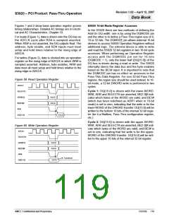
For reads (Figure 1), data is driven onto the DQ bus on
the ADCLK cycle after RD# is sampled asserted.
When RD# is not asserted, the DQ outputs float. The
address, byte enable, and RD# inputs must meet
setup and hold times relative to the rising edge of
ADCLK.
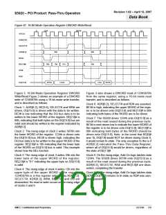
For writes (Figure 2), data is clocked into an operation
register on the rising edge of ADCLK in which WR# is
sampled asserted. Address, byte enables, WR# and
data must all meet setup and hold times relative to the
rising edge or ADCLK.
Figure 59. Read Operation Register
ADCLK
SELECT#
Cycle 1: DQ[15:0] is driven with the lower-WORD.
WR#, ADR and SELECT# are asserted, BE[1:0]# indi-
cates which bytes of the WORD are valid, and BE3#
(which has been redefined as ADR1 when in 16-bit
mode) is set to zero, indicating that the write is for the
lower-WORD of the DWORD transfer. DQ[15:0] will be
written to the bottom 16 bits of the internal 32-bit regis-
ter (be it a Mailbox, Pass-Thru configuration register,
etc.).
ADR[6:2]
BE[3:0]#
RD#
VALID
VALID
DQ[31:0]
VALID
Cycle 2: DQ[15:0] is driven with the upper-WORD.
WR#, ADR and SELECT# are asserted, BE[1:0]# indi-
cate which bytes of the WORD are valid, and BE3# is
set to one, indicating that the write is for the upper-
WORD of the DWORD transfer. DQ[15:0] will be writ-
ten to the upper 16-bits of the internal 32-bit register.
Figure 60. Write Operation Register
ADCLK
SELECT#
ADR[6:2]
BE[3:0]#
WR#
VALID
VALID
Transfered
DQ[31:0]
DATA
AMCC Confidential and Proprietary
DS1596
119

 AMCC [ APPLIED MICRO CIRCUITS CORPORATION ]