Revision J – April 7, 2006
S2004 – Quad Serial Backplane Device
Data Sheet
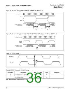
Table 21. S2004 Receiver Timing (Full and Half Clock Mode)
Parameters
Description
Min
Max
Units
Conditions
T3
2.5
3.0
X
ns
ns
ns
ns
1.25 Gbps/612.5 Mbps TMODE = 1
Data Setup w.r.t. ↑ RCxP/N
1.062 Gbps/531 Mbps TMODE = 1
1.25 Gbps/612.5 Mbps TMODE = 0
1.062 Gbps/531 Mbps TMODE = 0
X
T4
T5
2.5
X
ns
ns
TMODE = 1
TMODE = 0
Data Hold w.r.t. ↑ RCxP/N
Data Setup w.r.t. ↑ RCxP/N
2.5
3.0
ns
at 1.25 Gbps/612.5 Mbps TMODE = 1
1,2
at 1.062 Gbps/531 Mbps TMODE = 1
T6
T7
2.5
ns
TMODE = 1
Data Hold w.r.t. ↑ RCxP/N
Time from RCxP rise to RCxN rise
7.5
8.9
8.5
9.9
ns
ns
at 1.25 Gbps/612.5 Mbps
1,2
at 1.062 Gbps/531 Mbps
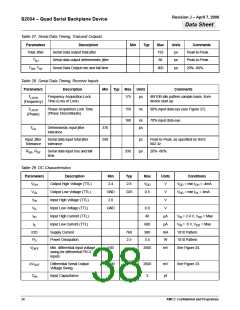
TRP, TFP
TRN, TFN
RCxP Rise and Fall Times
RCxN Rise and Fall Times
DOUTx Rise and Fall Times
RCxP/N Duty Cycle
2.4
2.4
2.4
60
ns
ns
ns
%
See Note 2. See Figure 22.
See Note 2. See Figure 22.
See Note 2. See Figure 22.
See Note 1.
TDR, TDF
Duty Cycle
40
1. Measurements made from the reference voltage levels of the clock (1.4V) to the valid input or output data levels (.8V or 2.0V).
2. TTL/CMOS AC timing measurements are assumed to have an output load of 10pf.
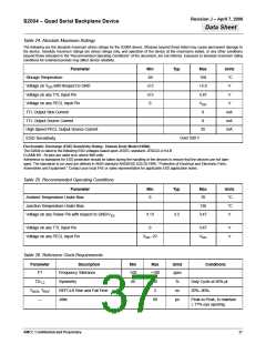
Table 22. Receiver Timing (External Clock Mode)
Parameters
Description
Min Max Units
3.0 8.0 ns
Conditions
T8
TCLKA to DOUTx
Propagation Delay
10pf load capacitance at the end of a 3-inch 50-Ω transmission
line.
Figure 18. Receiver Timing (Full Clock Mode, CMODE = 1)
SERIAL DATA IN
RCxN
RCxP
DOUTx[0:7], EOFx,
KFLAGx, ERRx
T3
T4
AMCC Confidential and Proprietary
35

 AMCC [ APPLIED MICRO CIRCUITS CORPORATION ]