Revision J – April 7, 2006
S2004 – Quad Serial Backplane Device
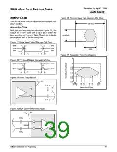
OUTPUT LOAD
Data Sheet
Figure 26. Receiver Input Eye Diagram Jitter Mask
The S2004 serial outputs do not require output pull-
down resistors.
Bit Time
Acquisition Time
With the input eye diagram shown in Figure 25, the
S2004 will recover data with a ≤1E-9 BER within the
Amplitude
time specified by T
in Table 28 after an instanta-
LOCK
neous phase shift of the incoming data.
Figure 22. Serial Input/Output Rise and Fall Time
80%
50%
20%
80%
50%
20%
24%
Tr
Tf
Figure 27. Acquisition Time Eye Diagram
1.3
Figure 23. TTL Input/Output Rise and Fall Time
+2.0V
+2.0V
+0.8V
1.0
0.8
0.7
+0.8V
Tr
Tf
0.5
0.3
0.2
Figure 24. Serial Output Load
VDD -2.3 V
0.0
0.01 µf
0.01 µf
Normalized Time
Figure 25. High Speed Differential Inputs
VDD - 1.3 V
0.01µf
100 Ω
0.01µf
AMCC Confidential and Proprietary
39

 AMCC [ APPLIED MICRO CIRCUITS CORPORATION ]