Features
■
■
■
■
■
Low-cost, low-power CPLD
Instant-on, non-volatile architecture
Standby current as low as 2 mA
Provides fast propagation delay and clock-to-output times
Provides four global clocks with two clocks available per logic array
block (LAB)
Features
■
■
UFM block up to 8 Kbits for non-volatile storage
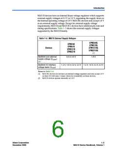
MultiVolt core enabling external supply voltages to the device of
either 3.3 V/2.5 V or 1.8 V
■
■
■
■
MultiVolt I/O interface supporting 3.3-V, 2.5-V, 1.8-V, and 1.5-V logic
levels
Bus-friendly architecture including programmable slew rate, drive
strength, bus-hold, and programmable pull-up resistors
Schmitt triggers enabling noise tolerant inputs (programmable per
pin)
Fully compliant with the Peripheral Component Interconnect Special
Interest Group (PCI SIG) PCI Local Bus Specification, Revision 2.2 for
3.3-V operation at 66 MHz
■
■
Supports hot-socketing
Built-in Joint Test Action Group (JTAG) boundary-scan test (BST)
circuitry compliant with IEEE Std. 1149.1-1990
ISP circuitry compliant with IEEE Std. 1532
■
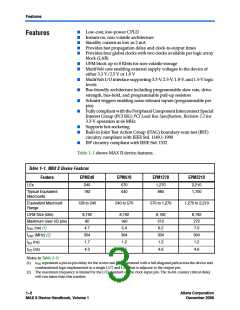
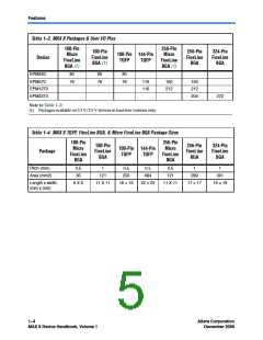
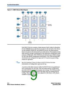
Table 1–1 shows MAX II device features.
Table 1–1. MAX II Device Features
Feature EPM240
EPM570
EPM1270
EPM2210
LEs
240
192
570
440
1,270
980
2,210
1,700
Typical Equivalent
Macrocells
Equivalent Macrocell
Range
128 to 240
240 to 570
570 to 1,270
1,270 to 2,210
UFM Size (bits)
Maximum User I/O pins
tPD1 (ns) (1)
8,192
80
8,192
160
5.4
8,192
212
6.2
8,192
272
7.0
4.7
f
t
t
CNT (MHz) (2)
SU (ns)
304
1.7
304
1.2
304
1.2
304
1.2
CO (ns)
4.3
4.5
4.6
4.6
Notes to Table 1–1:
(1) tPD1 represents a pin-to-pin delay for the worst case I/O placement with a full diagonal path across the device and
combinational logic implemented in a single LUT and LAB that is adjacent to the output pin.
(2) The maximum frequency is limited by the I/O standard on the clock input pin. The 16-bit counter critical delay
will run faster than this number.
1–2
Core Version a.b.c variable
Altera Corporation
December 2006
MAX II Device Handbook, Volume 1

 ALTERA [ ALTERA CORPORATION ]