Chapter 1. Introduction
MII51001-1.6
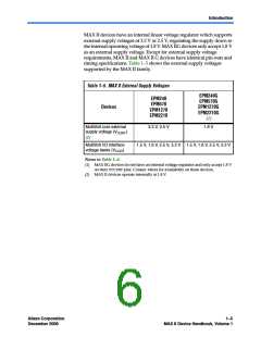
The MAX® II family of instant-on, non-volatile CPLDs is based on a
0.18-µm, 6-layer-metal-flash process, with densities from 240 to 2,210
logic elements (LEs) (128 to 2,210 equivalent macrocells) and non-volatile
storage of 8 Kbits. MAX II devices offer high I/O counts, fast
Introduction
performance, and reliable fitting versus other CPLD architectures.
Featuring MultiVolt™ core, a user flash memory (UFM) block, and
enhanced in-system programmability (ISP), MAX II devices are designed
to reduce cost and power while providing programmable solutions for
applications such as bus bridging, I/O expansion, power-on reset (POR)
and sequencing control, and device configuration control.
The following shows the main sections of the MAX II CPLD Family Data
Sheet:
Section
Page
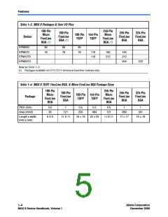
Features . . . . . . . . . . . . . . . . . . . . . . . . . . . . . . . . . . . . . . . . . . . . . 1–2
Functional Description . . . . . . . . . . . . . . . . . . . . . . . . . . . . . . . . 2–1
Logic Array Blocks. . . . . . . . . . . . . . . . . . . . . . . . . . . . . . . . . . . . 2–5
Logic Elements . . . . . . . . . . . . . . . . . . . . . . . . . . . . . . . . . . . . . . . 2–8
MultiTrack Interconnect . . . . . . . . . . . . . . . . . . . . . . . . . . . . . . 2–15
Global Signals. . . . . . . . . . . . . . . . . . . . . . . . . . . . . . . . . . . . . . . 2–20
User Flash Memory Block. . . . . . . . . . . . . . . . . . . . . . . . . . . . . 2–23
MultiVolt Core . . . . . . . . . . . . . . . . . . . . . . . . . . . . . . . . . . . . . . 2–27
I/O Structure . . . . . . . . . . . . . . . . . . . . . . . . . . . . . . . . . . . . . . . 2–28
IEEE Std. 1149.1 (JTAG) Boundary Scan Support. . . . . . . . . . 3–1
In System Programmability . . . . . . . . . . . . . . . . . . . . . . . . . . . . 3–4
Hot Socketing . . . . . . . . . . . . . . . . . . . . . . . . . . . . . . . . . . . . . . . . 4–1
Power-On Reset Circuitry. . . . . . . . . . . . . . . . . . . . . . . . . . . . . . 4–6
Operating Conditions . . . . . . . . . . . . . . . . . . . . . . . . . . . . . . . . . 5–1
Power Consumption . . . . . . . . . . . . . . . . . . . . . . . . . . . . . . . . . . 5–9
Timing Model & Specifications . . . . . . . . . . . . . . . . . . . . . . . . 5–10
Device Pin-Outs . . . . . . . . . . . . . . . . . . . . . . . . . . . . . . . . . . . . . . 6–1
Ordering Information . . . . . . . . . . . . . . . . . . . . . . . . . . . . . . . . . 6–1
Altera Corporation
December 2006
Core Version a.b.c variable
1–1
Preliminary

 ALTERA [ ALTERA CORPORATION ]