Chapter 17: Understanding and Evaluating Power in MAX II Devices
17–5
PowerPlay Early Power Estimator Inputs
Table 17–1. Input Parameter Section Information (Part 2 of 2)
Input Parameter
Description
VCCINT Supply
The voltage of the VCCINT power supply. For MAX IIG and MAX IIZ devices, the supply voltage must
be 1.8 V. For other devices, it can be either 2.5 V or 3.3 V. Devices with lower VCCINT have lower total
standby power consumption.
Ambient Temperature Enter the air temperature near the CPLD. This value can range from –40°C to 125°C, depending on
the device temperature grade. This parameter is used to compute junction temperature based on
power dissipation and thermal resistances through the top of the chip.
Airflow
Select an available ambient airflow in linear feet per minute (lfm) or meters per second (m/s). The
options are still air, 100 lfm (0.5 m/s), 200 lfm (1.0 m/s), or 400 lfm (2.0 m/s). Increased airflow
results in a lower junction-to-air thermal resistance, and thus lower junction temperature.
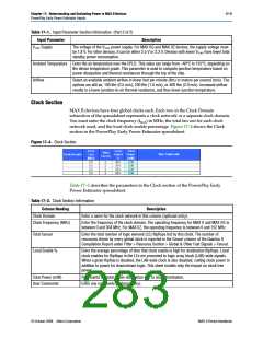
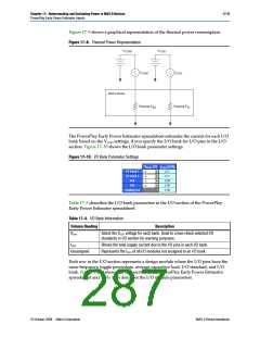
Clock Section
MAX II devices have four global clocks each. Each row in the Clock Domain
subsection of the spreadsheet represents a clock network or a separate clock domain.
You must enter the clock frequency (fMAX) in MHz, the total fan-out for each clock
network used, and the local clock enable percentage. Figure 17–4 shows the Clock
section in the PowerPlay Early Power Estimator spreadsheet.
Figure 17–4. Clock Section
Table 17–2 describes the parameters in the Clock section of the PowerPlay Early
Power Estimator spreadsheet.
Table 17–2. Clock Section Information
Column Heading
Clock Domain
Description
Enter a name for the clock network in this column (optional entry).
Clock Frequency (MHz)
Enter the frequency of the clock domain. The operating frequency for MAX II and MAX IIG is
between 0 and 304 MHz. For MAX IIZ, the operating frequency is between 0 and 152 MHz.
Total Fanout
Enter the total number of logic element (LE) flipflops fed by this clock. The number of
resources driven by every global clock is reported in the Fanout column of the Quartus II
Compilation Report under Fitter > Resource Section > Global & Other Fast Signals > Fanout.
Local Enable %
Enter the average percentage of time that clock enable is high for destination flipflops. Local
clock enables for flipflops in the LEs are promoted to logic array block (LAB)-wide signals.
When a given flipflop is disabled, the LAB-wide clock is also disabled, cutting clock power in
addition to power for downstream logic. This sheet models only the impact on clock tree
power.
Total Power (mW)
User Comments
Represents the total power dissipation due to clock distribution.
Enter any comments (optional entry).
© October 2008 Altera Corporation
MAX II Device Handbook

 ALTERA [ ALTERA CORPORATION ]