Chapter 4: Hot Socketing and Power-On Reset in MAX II Devices
4–5
Power-On Reset Circuitry
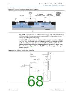
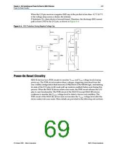
When the I/O pin receives a negative ESD zap at the pin that is less than –0.7 V (0.7 V
is the voltage drop across a diode), the intrinsic
P-Substrate/N+ drain diode is forward biased. Therefore, the discharge ESD current
path is from GND to the I/O pin, as shown in Figure 4–4.
Figure 4–4. ESD Protection During Negative Voltage Zap
I/O
Source
D
Gate
PMOS
N+
Drain
Drain
P-Substrate
G
I/O
S
Gate
N+
NMOS
Source
GND
GND
Power-On Reset Circuitry
MAX II devices have POR circuits to monitor VCCINT and VCCIO voltage levels during
power-up. The POR circuit monitors these voltages, triggering download from the
non-volatile configuration flash memory (CFM) block to the SRAM logic, maintaining
tri-state of the I/O pins (with weak pull-up resistors enabled) before and during this
process. When the MAX II device enters user mode, the POR circuit releases the I/O
pins to user functionality. The POR circuit of the MAX II (except MAX IIZ) device
continues to monitor the VCCINT voltage level to detect a brown-out condition. The
POR circuit of the MAX IIZ device does not monitor the VCCINT voltage level after the
device enters into user mode. More details are provided in the following sub-sections.
© October 2008 Altera Corporation
MAX II Device Handbook

 ALTERA [ ALTERA CORPORATION ]