1–34
Chapter 1: Cyclone IV Device Datasheet
Switching Characteristics
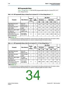
IOE Programmable Delay
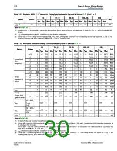
Table 1–40 and Table 1–41 list the IOE programmable delay for Cyclone IV E 1.0 V
core voltage devices.
Table 1–40. IOE Programmable Delay on Column Pins for Cyclone IV E 1.0 V Core Voltage Devices (1), (2)
Max Offset
Number
Min
Parameter
Paths Affected
of
Fast Corner
C8L I8L
Slow Corner
C9L
Unit
Offset
Setting
C8L
I8L
Input delay from pin to
internal cells
Pad to I/O
dataout to core
7
8
2
0
0
0
2.054 1.924 3.387 4.017 3.411
2.010 1.875 3.341 4.252 3.367
0.641 0.631 1.111 1.377 1.124
ns
ns
ns
Input delay from pin to
input register
Pad to I/O input
register
Delay from output register
to output pin
I/O output
register to pad
Input delay from
dual-purpose clock pin to
fan-out destinations
Pad to global
clock network
12
0
0.971 0.931 1.684 2.298 1.684
ns
Notes to Table 1–40:
(1) The incremental values for the settings are generally linear. For the exact values for each setting, use the latest version of the Quartus II software.
(2) The minimum and maximum offset timing numbers are in reference to setting 0 as available in the Quartus II software.
(2)
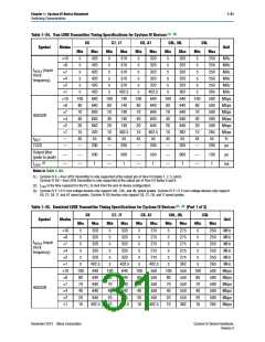
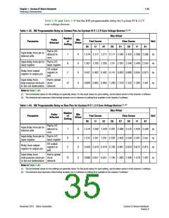
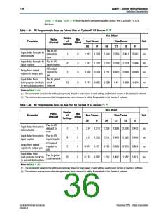
Table 1–41. IOE Programmable Delay on Row Pins for Cyclone IV E 1.0 V Core Voltage Devices (1),
Max Offset
Number
Min
Parameter
Paths Affected
of
Fast Corner
C8L I8L
Slow Corner
C9L
Unit
Offset
Setting
C8L
I8L
Input delay from pin to
internal cells
Pad to I/O
dataout to core
7
8
2
0
0
0
2.057 1.921 3.389 4.146 3.412
2.059 1.919 3.420 4.374 3.441
0.670 0.623 1.160 1.420 1.168
ns
ns
ns
Input delay from pin to
input register
Pad to I/O input
register
Delay from output register
to output pin
I/O output
register to pad
Input delay from
dual-purpose clock pin to
fan-out destinations
Pad to global
clock network
12
0
0.960 0.919 1.656 2.258 1.656
ns
Notes to Table 1–41:
(1) The incremental values for the settings are generally linear. For the exact values for each setting, use the latest version of the Quartus II software.
(2) The minimum and maximum offset timing numbers are in reference to setting 0 as available in the Quartus II software.
Cyclone IV Device Handbook,
Volume 3
December 2013 Altera Corporation

 ALTERA [ ALTERA CORPORATION ]