1–30
Chapter 1: Cyclone IV Device Datasheet
Switching Characteristics
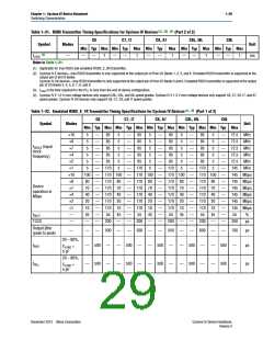
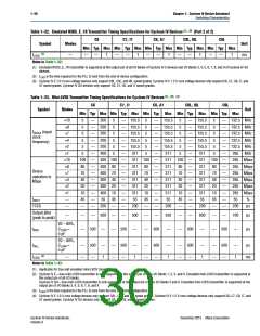
Table 1–32. Emulated RSDS_E_1R Transmitter Timing Specifications for Cyclone IV Devices (1), (3) (Part 2 of 2)
C6
C7, I7
C8, A7
C8L, I8L
C9L
Symbol
Modes
Unit
Min Typ Max Min Typ Max Min Typ Max Min Typ Max Min Typ Max
(2)
tLOCK
—
—
—
1
—
—
1
—
—
1
—
—
1
—
—
1
ms
Notes to Table 1–32:
(1) Emulated RSDS_E_1R transmitter is supported at the output pin of all I/O Banks of Cyclone IV E devices and I/O Banks 3, 4, 5, 6, 7, 8, and 9 of Cyclone IV GX
devices.
(2) tLOCK is the time required for the PLL to lock from the end-of-device configuration.
(3) Cyclone IV E 1.0 V core voltage devices only support C8L, C9L, and I8L speed grades. Cyclone IV E 1.2 V core voltage devices only support C6, C7, C8, I7, and
A7 speed grades. Cyclone IV GX devices only support C6, C7, C8, and I7 speed grades.
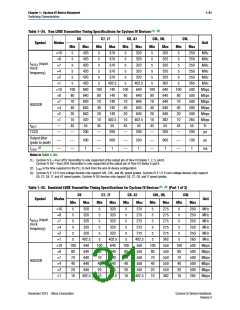
Table 1–33. Mini-LVDS Transmitter Timing Specifications for Cyclone IV Devices (1), (2), (4)
C6
C7, I7
C8, A7
C8L, I8L
C9L
Symbol
Modes
Unit
Min Typ Max Min Typ Max Min Typ Max Min Typ Max Min Typ Max
×10
×8
×7
×4
×2
×1
×10
×8
×7
×4
×2
×1
—
—
5
5
—
—
—
—
—
—
—
—
—
—
—
—
—
—
200
200
200
200
200
400
5
5
5
5
5
5
—
—
—
—
—
—
—
—
—
—
—
—
—
—
155.5
155.5
155.5
155.5
155.5
311
5
5
5
5
5
5
—
—
—
—
—
—
—
—
—
—
—
—
—
—
155.5
155.5
155.5
155.5
155.5
311
5
5
5
5
5
5
—
—
—
—
—
—
—
—
—
—
—
—
—
—
155.5
155.5
155.5
155.5
155.5
311
5
5
5
5
5
5
—
—
—
—
—
—
—
—
—
—
—
—
—
—
132.5 MHz
132.5 MHz
132.5 MHz
132.5 MHz
132.5 MHz
265 MHz
265 Mbps
265 Mbps
265 Mbps
265 Mbps
265 Mbps
265 Mbps
fHSCLK (input
clock
frequency)
5
5
5
5
100
80
70
40
20
10
45
—
400 100
400 80
400 70
400 40
400 20
400 10
311 100
311 100
311 100
311
311
311
311
311
55
80
70
40
20
10
45
—
311
311
311
311
311
55
80
70
40
20
10
45
—
311
311
311
311
311
55
80
70
40
20
10
45
—
Device
operation in
Mbps
tDUTY
55
45
—
55
%
TCCS
200
200
200
200
200
ps
Output jitter
(peak to peak)
—
—
—
500
—
—
500
—
—
550
—
—
600
—
—
700
ps
20 – 80%,
tRISE
CLOAD
5 pF
=
—
500
—
—
500
—
—
500
—
—
500
—
—
500
—
ps
20 – 80%,
tFALL
CLOAD
5 pF
=
—
—
500
—
—
1
—
—
500
—
—
1
—
—
500
—
—
1
—
—
500
—
—
1
—
—
500
—
—
1
ps
(3)
tLOCK
—
ms
Notes to Table 1–33:
(1) Applicable for true and emulated mini-LVDS transmitter.
(2) Cyclone IV E—true mini-LVDS transmitter is only supported at the output pin of Row I/O Banks 1, 2, 5, and 6. Emulated mini-LVDS transmitter is supported at
the output pin of all I/O banks.
Cyclone IV GX—true mini-LVDS transmitter is only supported at the output pin of Row I/O Banks 5 and 6. Emulated mini-LVDS transmitter is supported at the
output pin of I/O Banks 3, 4, 5, 6, 7, 8, and 9.
(3) tLOCK is the time required for the PLL to lock from the end-of-device configuration.
(4) Cyclone IV E 1.0 V core voltage devices only support C8L, C9L, and I8L speed grades. Cyclone IV E 1.2 V core voltage devices only support C6, C7, C8, I7, and
A7 speed grades. Cyclone IV GX devices only support C6, C7, C8, and I7 speed grades.
Cyclone IV Device Handbook,
Volume 3
December 2013 Altera Corporation

 ALTERA [ ALTERA CORPORATION ]