High-Speed Differential I/O Interfaces with DPA in Stratix II and Stratix II GX Devices
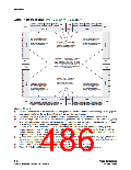
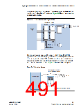
Figure 5–2. Stratix II GX I/O Banks Note (1), (2), (3), (4), (5), (6), and (7)
DQS ×8
DQS ×8
DQS ×8
DQS ×8
DQS ×8
DQS ×8
DQS ×8
DQS ×8
DQS ×8
PLL11
Bank 11
PLL5
PLL7 VREF0B3 VREF1B3 VREF2B3 VREF3B3 VREF4B3
Bank 3
VREF0B4 VREF1B4 VREF2B4 VREF3B4 VREF4B4
Bank 4
Bank 9
This I/O bank supports LVDS
and LVPECL standards
for input clock operations. Differential HSTL
and differential SSTL standards
are supported for both input
and output operations. (3)
This I/O bank supports LVDS
and LVPECL standards for input clock
operation. Differential HSTL and
differential SSTL standards are
supported for both input and output
operations. (3)
I/O Banks 3, 4, 9, and 11 support all single-ended
I/O standards for both input and output operations.
All differential I/O standards are supported for both
input and output operations at I/O banks 9 and 11.
I/O banks 1 & 2 support LVTTL, LVCMOS,
2.5 V, 1.8 V, 1.5 V, SSTL-2, SSTL-18 class I,
LVDS, pseudo-differential SSTL-2 and pseudo-differential
SSTL-18 class I standards for both input and output
operations. HSTL, SSTL-18 class II,
pseudo-differential HSTL and pseudo-differential
SSTL-18 class II standards are only supported for
input operations. (4)
PLL1
PLL2
I/O banks 7, 8, 10 and 12 support all single-ended I/O
standards for both input and output operations. All differential
I/O standards are supported for both input and output operations
at I/O banks 10 and 12.
This I/O bank supports LVDS
This I/O bank supports LVDS
and LVPECL standards for input clock operation.
Differential HSTL and differential
and LVPECL standards for input clock
operation. Differential HSTL and differential
SSTL standards are supported
SSTL standards are supported
for both input and output operations. (3)
for both input and output operations. (3)
Bank 8
Bank 7
Bank 12
PLL12
Bank 10
PLL6
VREF4B8 VREF3B8 VREF2B8 VREF1B8 VREF0B8
VREF4B7 VREF3B7 VREF2B7 VREF1B7 VREF0B7
PLL8
DQS ×8
DQS ×8
DQS ×8
DQS ×8
DQS ×8
DQS ×8
DQS ×8
DQS ×8
DQS ×8
Notes to Figure 5–2:
(1) Figure 5–2 is a top view of the silicon die which corresponds to a reverse view for flip-chip packages. It is a graphical
representation only.
(2) Depending on size of the device, different device members have different number of VREF groups. Refer to the pin
list and the Quartus II software for exact locations.
(3) Banks 9 through 12 are enhanced PLL external clock output banks.
(4) Horizontal I/O banks feature transceiver and DPA circuitry for high speed differential I/O standards.
(5) Quartus II software does not support differential SSTL and differential HSTL standards at left/right I/O banks.
Refer to the “Differential Pin Placement Guidelines” on page 5–21 if you need to implement these standards at these
I/O banks.
(6) Banks 11 and 12 are available only in EP2SGX60C/D/E, EP2SGX90E/F, and EP2SGX130G.
(7) PLLs 7, 8, 11, and 12 are available only in EP2SGX60C/D/E, EP2SGXE/F, and EP2SGX130G.
Altera Corporation
January 2008
5–3
Stratix II Device Handbook, Volume 2

 ALTERA [ ALTERA CORPORATION ]