5. High-Speed Differential I/O
Interfaces with DPA in Stratix II
and Stratix II GX Devices
SII52005-2.2
Stratix® II and Stratix® II GX device family offers up to 1-Gbps
differential I/O capabilities to support source-synchronous
communication protocols such as HyperTransport™ technology, Rapid
I/O, XSBI, and SPI.
Introduction
Stratix II and Stratix II GX devices have the following dedicated circuitry
for high-speed differential I/O support:
■
■
■
■
■
■
■
Differential I/O buffer
Transmit serializer
Receive deserializer
Data realignment circuit
Dynamic phase aligner (DPA)
Synchronizer (FIFO buffer)
Analog PLLs (fast PLLs)
For high-speed differential interfaces, Stratix II and Stratix II GX devices
can accommodate different differential I/O standards, including the
following:
■
■
■
■
■
LVDS
HyperTransport technology
HSTL
SSTL
LVPECL
1
HSTL, SSTL, and LVPECL I/O standards can be used only for
PLL clock inputs and outputs in differential mode.
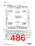
Stratix II and Stratix II GX inputs and outputs are partitioned into banks
located on the periphery of the die. The inputs and outputs that support
LVDS and HyperTransport technology are located in row I/O banks, two
on the left and two on the right side of the Stratix II device and two on the
left side of the Stratix II GX device. LVPECL, HSTL, and SSTL standards
are supported on certain top and bottom banks of the die (banks 9 to 12)
when used as differential clock inputs/outputs. Differential HSTL and
SSTL standards can be supported on banks 3, 4, 7, and 8 if the pins on
these banks are used as DQS/DQSn pins. Figures 5–1 and 5–2 show
where the banks and the PLLs are located on the die.
I/O Banks
Altera Corporation
January 2008
5–1

 ALTERA [ ALTERA CORPORATION ]