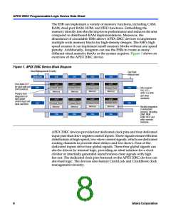
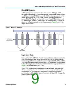
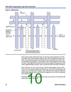
APEX 20KC Programmable Logic Device Data Sheet
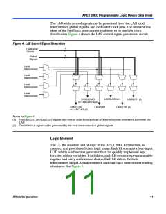
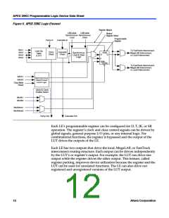
Figure 5. APEX 20KC Logic Element
Register Bypass
Packed
LAB-wide
Synchronous
Load
LAB-wide
Synchronous
Clear
Register Select
Programmable
Register
Carry-In
Cascade-In
data1
data2
data3
data4
To FastTrack Interconnect,
MegaLAB Interconnect,
or Local Interconnect
Look-Up
Table
(LUT)
Carry
Chain
Cascade
Chain
Synchronous
Load & Clear
Logic
PRN
D
Q
ENA
CLRN
To FastTrack Interconnect,
MegaLAB Interconnect,
or Local Interconnect
labclr1
labclr2
Asynchronous
Clear/Preset/
Load Logic
Chip-Wide
Reset
Clock & Clock
Enable Select
labclk1
labclk2
labclkena1
labclkena2
Carry-Out
Cascade-Out
Each LE’s programmable register can be configured for D, T, JK, or SR
operation. The register’s clock and clear control signals can be driven by
global signals, general-purpose I/O pins, or any internal logic. For
combinatorial functions, the register is bypassed and the output of the
LUT drives the outputs of the LE.
Each LE has two outputs that drive the local, MegaLAB, or FastTrack
interconnect routing structure. Each output can be driven independently
by the LUT’s or register’s output. For example, the LUT can drive one
output while the register drives the other output. This feature, called
register packing, improves device utilization because the register and the
LUT can be used for unrelated functions. The LE can also drive out
registered and unregistered versions of the LUT output.
12
Altera Corporation

 ALTERA [ ALTERA CORPORATION ]