AS29F400
Preliminary information
®
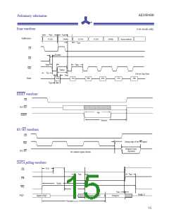
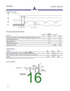
Toggle bit waveform
CE
t
OEH
WE
OE
DQ6
t
t
OE
DH
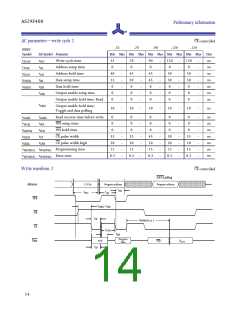
Erase and programming performance
Limits
Typical
1.0
15
Parameter
Min
Max
Unit
sec
Sector erase and verify-1 time (excludes 00h programming prior to erase)
Word programming time
-
-
-
-
µs
Byte program time
-
-
-
15
-
-
µs
Chip programming time
2.5
-
sec
Erase program cycles
10,000
cycles
Latchup tolerance
Parameter
Min
Max
+13.0
+1.0
Unit
Input voltage with respect to V on A9, OE, and RESET pin
-1.0
-1.0
-100
V
SS
Input voltage with respect to V on all DQ, address and control pins
V
V
SS
CC
Current
+100
mA
Includes all pins except VCC. Test conditions: VCC = 5.0V, one pin at a time.
AC test conditions
+5.0V
1N3064
or equivalent
2.7KΩ
Device under test
6.2KΩ
100 pF*
1N3064
or equivalent
VSS
VSS
*including scope
and jig capacitance
VSS
16

 ALSC [ ALLIANCE SEMICONDUCTOR CORPORATION ]