AS29F400
Preliminary information
®
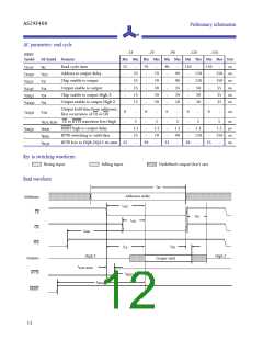
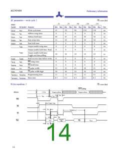
AC parameters: read cycle
-55
-70
-90
-120
-150
JEDEC
Symbol
Std Symbol Parameter
Min Max Min Max Min Max Min Max Min Max Unit
t
t
t
t
t
t
t
t
t
t
t
t
Read cycle time
55
-
-
70
-
-
90
-
-
120
-
150
-
ns
AVAV
AVQV
ELQV
GLQV
EHQZ
GHQZ
RC
ACC
CE
Address to output delay
Chip enable to output
55
55
25
15
15
70
70
30
20
20
90
90
35
20
20
-
-
-
-
-
120
120
50
-
-
-
-
-
150 ns
150 ns
-
-
-
Output enable to output
Chip enable to output High Z
Output enable to output High Z
-
-
-
55
35
35
ns
ns
ns
OE
DF
DF
-
-
-
30
-
-
-
30
Output hold time from addresses,
first occurrence of CE or OE
t
t
0
-
0
-
0
-
0
-
0
-
ns
ns
AXQX
OH
t
t
t
t
CE to BYTE transition low/high
RESET high to output delay
BYTE switching to valid data
-
-
-
5
1.5
55
-
-
-
5
1.5
70
-
-
-
5
1.5
90
-
-
-
5
1.5
120
-
-
-
5
ELFL/ELFH
t
1.5 µs
150 ns
PHQV
PWH
-
-
-
-
BDEL
BYTE low to DQ8–DQ15 tri-state 25
30
35
50
55
-
ns
FLQZ
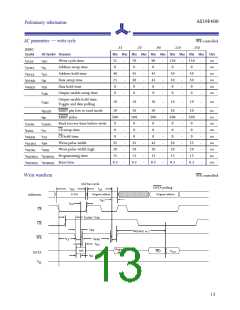
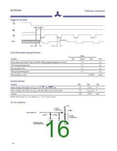
Key to switching waveforms
Rising input
Falling input
Undefined output/don’t care
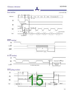
Read waveform
t
RC
Addresses stable
Addresses
CE
t
ACC
t
DF
t
OE
OE
t
OEH
WE
Outputs
BYTE
t
t
OH
CE
High Z
High Z
Output valid
t
ELFL/ELFH
t
BDEL
t
PWH
RESET
12

 ALSC [ ALLIANCE SEMICONDUCTOR CORPORATION ]