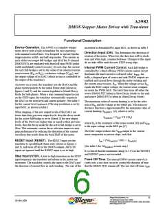
A3982
DMOS Stepper Motor Driver with Translator
is determined by the selection of an external resistor con-
Enable Input (ENABLE). This input turns on or off all
of the DMOS outputs. When set to a logic high, the outputs
are disabled. When set to a logic low, the internal control
enables the outputs as required. The translator inputs STEP,
DIR, and MS1, as well as the internal sequencing logic, all
remain active, independent of the ENABLE input state.
nected from the ROSC timing pin to ground. If the ROSC
pin is tied to an external voltage > 3 V, then tOFF defaults to
30 μs. The ROSC pin can be safely connected to the VDD
pin for this purpose. The value of tOFF (μs) is approximately
tOFF ≈ ROSC ⁄ 825
Shutdown. In the event of a fault, overtemperature
(excess TJ) or an undervoltage (on VCP), the DMOS out-
puts of the A3982 are disabled until the fault condition is
removed. At power-on, the UVLO (undervoltage lockout)
circuit disables the DMOS outputs and resets the translator
to the Home state.
Blanking. This function blanks the output of the current
sense comparators when the outputs are switched by the
internal current control circuitry. The comparator outputs
are blanked to prevent false overcurrent detection due to
reverse recovery currents of the clamp diodes, and switching
transients related to the capacitance of the load. The blank
time, tBLANK (μs), is approximately
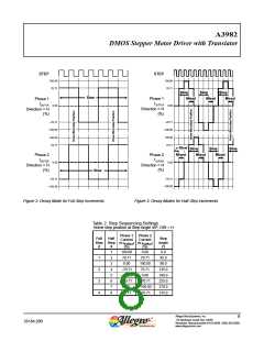
Mixed Decay Operation. The bridge can operate in
Mixed Decay Mode, depending on the step sequence, as
shown in figures 3 thru 5. As the trip point is reached, the
A3982 initially goes into a fast decay mode for 31.25%
of the off-time, tOFF. After that, it switches to Slow Decay
tBLANK ≈ 1 μs
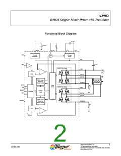
Charge Pump (CP1 and CP2). The charge pump is
used to generate a gate supply greater than that of VBB
for driving the source-side DMOS gates. A 0.1 μF ceramic
capacitor, should be connected between CP1 and CP2. In
addition, a 0.1 μF ceramic capacitor is required between
VCP and VBB, to act as a reservoir for operating the
high-side DMOS gates.
Mode for the remainder of tOFF
.
Synchronous Rectification. When a PWM-off cycle
is triggered by an internal fixed–off-time cycle, load current
recirculates according to the decay mode selected by the
control logic. This synchronous rectification feature turns on
the appropriate FETs during current decay, and effectively
shorts out the body diodes with the low DMOS RDSON. This
reduces power dissipation significantly, and can eliminate
the need for external Schottky diodes in many applications.
Turning off synchronous rectification prevents the reversal of
the load current when a zero-current level is detected.
VREG (VREG). This internally-generated voltage is
used to operate the sink-side DMOS outputs. The VREG
pin must be decoupled with a 0.22 μF ceramic capacitor to
ground. VREG is internally monitored. In the case of a fault
condition, the DMOS outputs of the A3982 are disabled.
Allegro MicroSystems, Inc.
7
115 Northeast Cutoff, Box 15036
26184.28B
Worcester, Massachusetts 01615-0036 (508) 853-5000
www.allegromicro.com

 ALLEGRO [ ALLEGRO MICROSYSTEMS ]