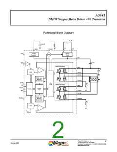
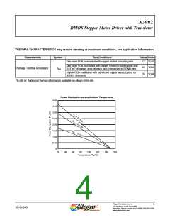
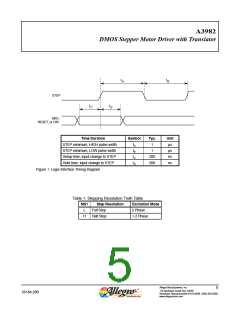
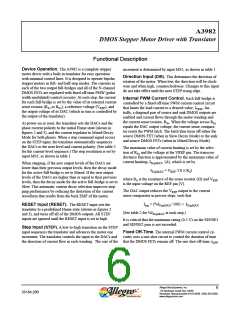
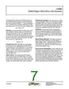
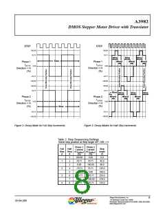
A3982
DMOS Stepper Motor Driver with Translator
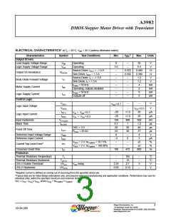
ELECTRICAL CHARACTERISTICS1 at TA = 25°C, VBB = 35 V (unless otherwise noted)
2
Characteristics
Output Drivers
Symbol
Test Conditions
Min.
Max.
Units
Typ.
Load Supply Voltage Range
Logic Supply Voltage Range
VBB
VDD
Operating
8
3.0
–
–
–
35
5.5
0.460
0.380
1.2
1.2
4
V
V
Operating
Source Driver, IOUT = –1.5 A
Sink Driver, IOUT = 1.5 A
Source Diode, IF = –1.5 A
Sink Diode, IF = 1.5 A
fPWM < 50 kHz
0.370
Ω
Output On Resistance
Body Diode Forward Voltage
Motor Supply Current
RDSON
VF
–
0.330
Ω
–
–
–
–
–
–
–
V
–
V
–
mA
mA
mA
mA
IBB
Operating, outputs disabled
fPWM < 50 kHz
–
2
–
8
Logic Supply Current
IDD
Outputs off
–
5
Control Logic
VIN(1)
–
–
V
VDD×0.7
–
Logic Input Voltage
Logic Input Current
VIN(0)
IIN(1)
IIN(0)
–
V
VDD×0.3
–20
<1.0
<1.0
20
μA
μA
VIN = VDD×0.7
VIN = VDD×0.3
–20
20
Input Hysteresis
Blank Time
VHYS(IN)
tBLANK
150
0.7
20
23
0
300
1
500
1.3
40
37
4
mV
μs
μs
μs
V
OSC > 3 V
30
30
–
Fixed Off-Time
tOFF
ROSC = 25 kΩ
Reference Input Voltage Range
Reference Input Current
VREF
IREF
–3
–
0
3
μA
%
VREF = 2 V, %ITripMAX = 70.71%
VREF = 2 V, %ITripMAX = 100.00%
–
±5
±5
800
Current Trip-Level Error3
errI
tDT
–
–
%
Crossover Dead Time
Protection
100
475
ns
Thermal Shutdown Temperature
Thermal Shutdown Hysteresis
UVLO Enable Threshold
UVLO Hysteresis
TJ
–
165
15
–
–
3
–
°C
°C
V
TJHYS
UVLO
UVHYS
–
VDD rising
2.35
0.05
2.7
0.10
V
1
2
Negative current is defined as coming out of (sourcing from) the specified device pin.
Typical data are for initial design estimations only, and assume optimum manufacturing and application conditions. Performance may vary for
individual units, within the specified maximum and minimum limits.
3errI = (ITrip – IProg) ⁄ IProg, where IProg = %ITripMAX
I
.
×
TripMAX
Allegro MicroSystems, Inc.
3
115 Northeast Cutoff, Box 15036
26184.28B
Worcester, Massachusetts 01615-0036 (508) 853-5000
www.allegromicro.com

 ALLEGRO [ ALLEGRO MICROSYSTEMS ]