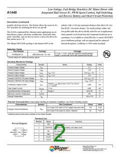
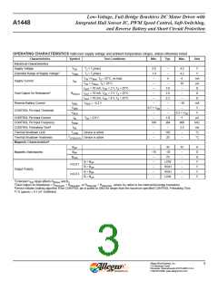
Low-Voltage, Full-Bridge Brushless DC Motor Driver with
Integrated Hall Sensor IC, PWM Speed Control, Soft-Switching,
and Reverse Battery and Short Circuit Protection
A1448
Power Derating
The device must be operated below the maximum junction tem-
perature of the device, TJ (max). Under certain combinations of
peak conditions, reliable operation may require derating supplied
power or improving the heat dissipation properties of the appli-
cation. This section presents a procedure for correlating factors
affecting operating TJ. (Thermal data is also available on the
Allegro MicroSystems website.)
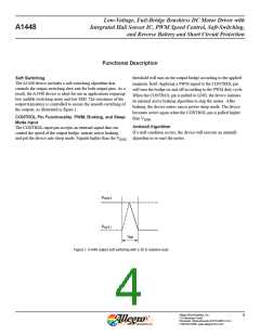
For a load of 30 Ω, and given common conditions such as:
TA= 25°C, VDD = 3 V, IDD = 83 mA, VLOAD = 2.43 V,
ILOAD = 81 mA, and RθJA = 125 °C/W, (see figure 5)
then:
PD = VDD × IDD – VLOAD × ILOAD
= 3 V × 83 mA – 2.43 V × 81 mA
= 52.17 mW
The package thermal resistance, RθJA, is a figure of merit sum-
marizing the ability of the application and the device to dissipate
heat from the junction (die), through all paths to the ambient air.
Its primary component is the effective thermal conductivity, K, of
the printed circuit board, including adjacent devices and traces.
Radiation from the die through the device case, RθJC, is relatively
small component of RθJA. Ambient air temperature, TA, and air
motion are significant external factors, damped by overmolding.
ΔT = PD × RθJA
= 52.17 mW × 125 °C/W
= 7°C
The effect of varying power levels (Power Dissipation, PD), can
be estimated. The following formulas represent the fundamental
relationships used to estimate TJ, at various PD levels.
TJ = TA + ΔT
= 25°C + 7°C
= 32°C
PD = VIN × IIN
ΔT = PD × RθJA
TJ = TA + ΔT
(1)
(2)
(3)
A worst-case estimate, PD(max), represents the maximum allow-
able power level, without exceeding TJ(max), at a selected RθJA
and TA.
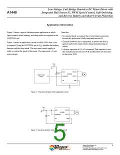
VBATT
VDD
VOUT2
A1448
M
VOUT1
GND
CONTROL
CBYP
NC
Figure 5. A1448 typical application
Allegro MicroSystems, Inc.
115 Northeast Cutoff
6
Worcester, Massachusetts 01615-0036 U.S.A.
1.508.853.5000; www.allegromicro.com

 ALLEGRO [ ALLEGRO MICROSYSTEMS ]