Low-Voltage, Full-Bridge Brushless DC Motor Driver with
Integrated Hall Sensor IC, PWM Speed Control, Soft-Switching,
and Reverse Battery and Short Circuit Protection
A1448
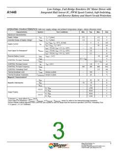
OPERATING CHARACTERISTICS Valid over supply voltage and ambient temperature ranges, unless otherwise noted
Characteristics
Electrical Characteristics
Supply Voltage
Symbol
Test Conditions
Min.
Typ.
Max.
Unit
VDD
TJ < TJ(max)
TJ < TJ(max)
2.0
–
–
4.2
V
V
Extended Range of Supply Voltage1
VDDE
1.8
4.2
VIN >VINHI , TA = 25°C, no load
IN < VINLO , TA = 25°C
IOUT = 70 mA, VDD = 2 V, TA = 25°C
OUT = 70 mA, VDD = 3 V, TA = 25°C
–
4
6
mA
μA
Ω
Supply Current
IDD
V
–
–
10
–
3.9
2.6
2.2
–
–
Total Output On-Resistance2
RDS(on)
I
–
–
Ω
IOUT = 70 mA, VDD = 4 V, TA = 25°C
VRDD = –4.2 V
–
–
Ω
Reverse Battery Current
IRDD
VINHI
VINLO
IIN
–
–10
mA
V
0.7 × VDD
–
–
CONTROL Pin Input Threshold
–
–
–
0.2 × VDD
V
CONTROL Pin Input Current
CONTROL Pin Input Frequency
CONTROL Prebraking Time3
Thermal Shutdown Limit
VIN = 3.0 V
1.0
384
–
5
800
2.5
–
μA
kHz
ms
°C
°C
fPWM
tPB
100
–
TJTSD
Device is active
–
165
20
Thermal Shutdown Hysteresis
Magnetic Characteristics4
TJTSD(HYS) Device is active
–
–
BOP
BRP
–
–75
–
35
75
–
G
G
G
V
V
V
V
Magnetic Switchpoints
–35
BHYS
70
–
B < BRP
VOUT1
–
LOW
HIGH
HIGH
LOW
–
B > BOP
–
–
Output Polarity
B < BRP
VOUT2
–
–
B > BOP
–
–
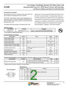
1Extended VDD range affects RDS(on) and Bx.
2Total Output On-Resistance = RDS(on)Q1 + RDS(on)Q4 , or RDS(on)Q2 + RDS(on)Q3 , where Qx refers to the internal full-bridge transistors.
3Device initiates braking algorithm if the CONTROL pin is pulled to GND for longer than the maximum specified CONTROL Prebraking Time.
41 G (gauss) = 0.1 mT (millitesla).
Allegro MicroSystems, Inc.
115 Northeast Cutoff
3
Worcester, Massachusetts 01615-0036 U.S.A.
1.508.853.5000; www.allegromicro.com

 ALLEGRO [ ALLEGRO MICROSYSTEMS ]