Low-Voltage, Full-Bridge Brushless DC Motor Driver with
Integrated Hall Sensor IC, PWM Speed Control, Soft-Switching,
and Reverse Battery and Short Circuit Protection
A1448
Description (continued)
portable electronic devices. This feature allows the removal of a
FET transistor for switching the device on and off.
industry with a 0.40 mm maximum thickness that allows for very
thin BLDC coin motor designs. The small package outline and
low profile make this device ideally suited for use in applications
where printed circuit board area and component headroom are at
a premium. It is available in a lead (Pb) free, 6-contact MLP/DFN
micro-leadframe package, with an exposed pad for enhanced
thermal dissipation. Leadframe is 100% matte tin plated.
The A1448 is optimized for vibration motor applications in cel-
lular phones, pagers, electronic toothbrushes, hand-held video
game controllers, and can also be used as a micro-fan driver for
fans motors up to 1 W.
The Allegro DFN (EW) package is the thinnest DFN in the
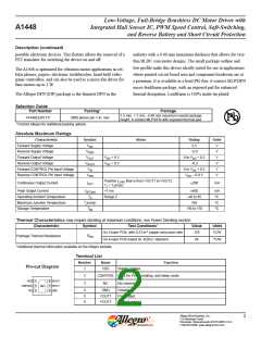
Selection Guide
Part Number
Packing*
Package
1.5 mm × 2 mm , 0.40 mm maximum overall package
height, 6-contact MLP/DFN with exposed thermal pad
A1448EEWLT-P
3000 pieces per 7-in. reel
*Contact Allegro for additional packing options
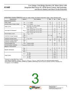
Absolute Maximum Ratings
Characteristic
Symbol
Notes
Rating
5.5
Units
Forward Supply Voltage
VDD
VRDD
VOUT
VROUT
VIN
V
V
V
V
V
V
Reverse Supply Voltage
–5.0
Forward Output Voltage
VDD > 0 V
VDD > 0 V
0 to VDD + 0.3
–0.3
Reverse Output Voltage
Forward CONTROL Pin Input Voltage
Reverse CONTROL Pin Input Voltage
0 to VDD + 0.3
VDD – 6.0 V
VRIN
Positive ILOAD flow is from VOUT1 to VOUT2,
TJ < TJ(max)
Continuous Output Current
IOUT
±200
mA
Peak Output Current
IOUT(pk)
TA
<1 ms
±400
–40 to 85
165
mA
ºC
ºC
ºC
Operating Ambient Temperature
Maximum Junction Temperature
Storage Temperature
Range E
TJ(max)
Tstg
–65 to 170
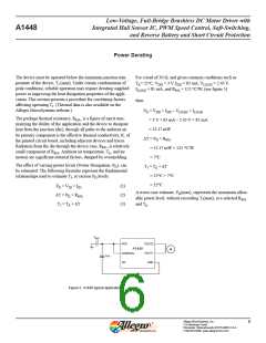
Thermal Characteristics may require derating at maximum conditions, see Power Derating section
Characteristic
Symbol
Test Conditions*
Value
Units
On 2-layer PCB, with 0.23 in.2 copper area each side
125
ºC/W
Package Thermal Resistance
RθJA
On 4-layer PCB based on JEDEC standard
64
ºC/W
*Additional thermal information available on the Allegro website
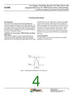
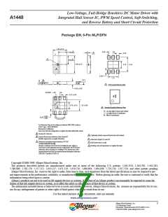
Terminal List
Number
Name
Function
Pin-out Diagram
1
VDD
Supply voltage
2
3
CONTROL Input for PWM, braking, and sleep mode
VDD
CONTROL
NC
1
2
3
6
5
4
VOUT2
VOUT1
GND
NC
No connection
PAD
4
5
6
GND
Ground
VOUT1
VOUT2
First output
Second output
Allegro MicroSystems, Inc.
115 Northeast Cutoff
2
Worcester, Massachusetts 01615-0036 U.S.A.
1.508.853.5000; www.allegromicro.com

 ALLEGRO [ ALLEGRO MICROSYSTEMS ]