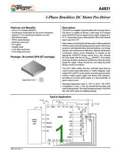
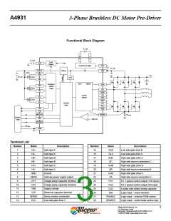
A4931
3-Phase Brushless DC Motor Pre-Driver
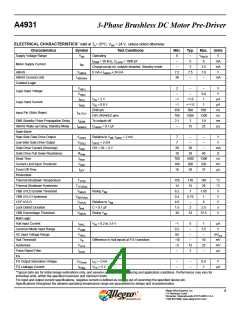
ELECTRICAL CHARACTERISTICS* Valid at TA= 25°C, VBB = 24 V, unless noted otherwise
Characteristics
Symbol
Test Conditions
Min.
8
Typ.
Max.
VBBOV
6
Units
V
Supply Voltage Range
VBB
Operating
–
5
fPWM < 30 kHz, CLOAD = 1000 pF
Charge pump on, outputs disabled, Standby mode
0 mA ≤ IHBIAS ≤ 24 mA
–
mA
mA
V
Motor Supply Current
IBB
–
3
3.5
HBIAS
VHBIAS
7.2
30
7.5
–
7.8
HBIAS Current Limit
Control Logic
IHBIASlim
–
mA
VIN(1)
VIN(0)
IIN(1)
2
–
–
–
–
0.8
1
V
V
Logic Input Voltage
Logic Input Current
Input Pin Glitch Reject
VIN = 2 V
–1
–1
350
700
2.1
–
<1.0
<–1.0
500
1000
3
μA
μA
ns
ns
ms
μs
IIN(0)
VIN = 0.8 V
1
ENB pin
650
1300
3.9
25
tGLITCH
DIR, BRAKEZ pins
To outputs off
CHBIAS = 0.1 μF
ENB Standby Pulse Propagation Delay
HBIAS Wake-up Delay, Standby Mode
Gate Drive
tdENB
tdHBIAS
15
High-Side Gate Drive Output
Low-Side Gate Drive Output
Gate Drive Current (Sourcing)
Gate Drive Pull Down Resistance
Dead Time
VGS(H)
VGS(L)
IGate
Relative to VBB, IGATE = 2 mA
IGATE = 2 mA
7
7
–
–
–
–
V
V
GH = GL = 4 V
20
10
700
180
18
30
–
mA
Ω
RGate
tdead
VREF
tOFF
28
40
1000
200
28
1300
220
37
ns
mV
μs
Current Limit Input Threshold
Fixed Off-Time
Protection
Thermal Shutdown Temperature
Thermal Shutdown Hysteresis
VBB UVLO Enable Threshold
VBB UVLO Hysteresis
VCP UVLO
TJTSD
TJTSDhys
VBBUV
VBBUVhys
VCPUV
tlock
155
14
170
15
7
185
26
°C
°C
V
Rising VBB
6.2
0.4
4.6
1.5
30
7.85
1
0.75
–
V
Relative to VBB
C = 0.1 μF
6
V
Lock Detect Duration
VBB Overvoltage Threshold
Hall Logic
2
2.5
37.5
s
VBBOV
Rising VBB
33
V
Hall Input Current
IHALL
VCMR
VHALL
Vth
VIN = 0.2 to 3.5 V
–1
0.2
60
–10
–5
–
0
–
1
3.5
–
μA
V
Common Mode Input Range
AC Input Voltage Range
Hall Threshold
–
mVp-p
mV
mV
μs
Difference in Hall inputs at FG1 transition
–
10
25
–
Hysteresis
VHYS
tpulse
12
2
Pulse Reject Filter
FG
FG Output Saturation Voltage
FG Leakage Current
VFG(sat)
IFGlkg
IFG = 2 mA
VFG = 5 V
–
–
–
–
0.5
1
V
μA
*Typical data are for initial design estimations only, and assume optimum manufacturing and application conditions. Performance may vary for
individual units, within the specified maximum and minimum limits.
For input and output current specifications, negative current is defined as coming out of (sourcing) the specified device pin.
Specifications throughout the allowed operating temperature range are guaranteed by design and characterization.
Allegro MicroSystems, Inc.
115 Northeast Cutoff
4
Worcester, Massachusetts 01615-0036 U.S.A.
1.508.853.5000; www.allegromicro.com

 ALLEGRO [ ALLEGRO MICROSYSTEMS ]