[AK8975/C]
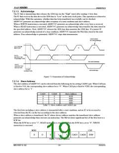
7.2.1.3. Acknowledge
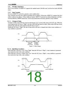
The IC that is transmitting data releases the SDA line (in the "High" state) after sending 1-byte data.
The IC that receives the data drives the SDAline to "Low" on the next clock pulse. This operation is referred to
acknowledge. With this operation, whether data has been transferred successfully can be checked.
AK8975/C generates an acknowledge after reception of a start condition and slave address.
When a WRITE instruction is executed, AK8975/C generates an acknowledge after every byte is received.
When a READ instruction is executed, AK8975/C generates an acknowledge then transfers the data stored at
the specified address. Next, AK8975/C releases the SDA line then monitors the SDA line. If a master IC
generates an acknowledge instead of a stop condition, AK8975/C transmits the 8bit data stored at the next
address. If no acknowledge is generated, AK8975/C stops data transmission.
Clock pulse
for acknowledge
SCL FROM
MASTER
1
8
9
DATA
OUTPUT BY
TRANSMITTER
not acknowledge
acknowledge
DATA
OUTPUT BY
RECEIVER
START
CONDITION
Figure 7.5 Generation of Acknowledge
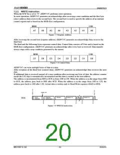
7.2.1.4. Slave Address
The slave address of AK8975/C can be selected from the following list by setting CAD0/1 pin. When CAD pin
is fixed to VSS, the corresponding slave address bit is “0”. When CAD pin is fixed to VDD, the corresponding
slave address bit is “1”.
CAD1
CAD0
Slave Address
0CH
0
0
1
1
0
1
0
1
0DH
0EH
0FH
Table 7.1 Slave Address and CAD0/1 pin
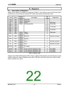
The first byte including a slave address is transmitted after a start condition, and an IC to be accessed is
selected from the ICs on the bus according to the slave address.
When a slave address is transferred, the IC whose device address matches the transferred slave address
generates an acknowledge then executes an instruction. The 8th bit (least significant bit) of the first byte is a
R/W bit.
When the R/W bit is set to "1", READ instruction is executed. When the R/W bit is set to "0", WRITE
instruction is executed.
MSB
0
LSB
R/W
0
0
1
1
CAD1 CAD0
Figure 7.6 Slave Address
MS1187-E-02
- 19 -
2010/05

 AKM [ ASAHI KASEI MICROSYSTEMS ]