[ASAHI KASEI]
[AK7740ET]
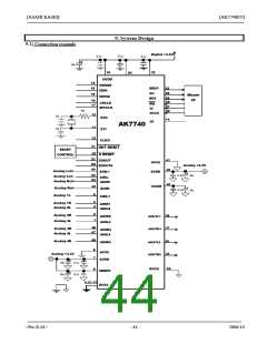
9-2) Peripheral circuit
9-2-3) Ground and power supply
To minimize digital noise coupling, AVDD and DVDD should be individually de-coupled at the AK7740. System
analog power is supplied to AVDD. Generally, power supply and ground wires must be connected separately
according to the analog and digital systems. Connect them at a position close to the power source on the PC board.
Decoupling capacitors, and ceramic capacitors of small values in particular, should be connected at positions as close
as possible to the AK7740.
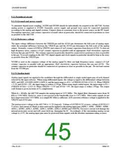
9-2-4) Reference voltage
The input voltage difference between the VREFH pin and the AVSS pin determines the full scale of analog input,
while the potential difference between the VREFH pin and the AVSS pin determines the full scale of the analog
output. Normally, connect AVDD to VREFH, and connect 0.1µF ceramic capacitors from them to AVSS. To shut out
high frequency noise, connect a 0.1µF ceramic capacitor in parallel with an appropriate 10µF electrolytic capacitor
between this pin and AVSS. The ceramic capacitor in particular should be connected at a position as close as possible
to the pin. To avoid coupling to the AK7740, digital signals and clock signals in particular should be kept as far away
as possible from the VREFH pin.
VCOM is used as the common voltage of the analog signal.To filter out high frequency noise, connect a 0.1µF
ceramic capacitor in parallel with an appropriate 10µF electrolytic capacitor between this pin and AVSS. The
ceramic capacitor in particular should be connected at a position as close as possible to the pin. Do not lead current
from the VCOM pin.
9-2-5) Analog input
Analog input signals are applied to the modulator through the differential or single-ended input pins of each channel
selected by the input selector. When using differential inputs, the voltage is equal to the differential voltage between
AIN+ and AIN- (∆VAIN=(AIN+)-(AIN-)), and the input range is ±FS = ±(VREFH-AVSS)×(2.0/3.3). When VREFH
= 3.3V and AVSS = 0V, the input range is within ±2.0Vpp. When using single-ended inputs, the input range is FS =
(VREFH-AVSS) × (2.0/3.3). When VREFH = 3.3V and AVSS = 0V, the input range is within 2.0Vpp. The output
code format is given in terms of 2's complements.
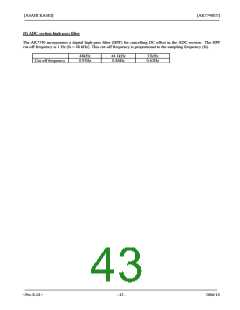
When fs = 48 kHz, the AK7740 samples the analog input at 3.072 MHz. The digital filter eliminates noise from 30
kHz to 3.042 MHz. However, noise is not rejected in the bandwidth close to 3.072 MHz. Most audio signals do not
have large noise near 3.072 MHz, so a simple RC filter is sufficient. A/D converter reference voltage is applied to the
VREFH and AVSS pins.
The analog source voltage to the AK7740 is +3.3V (typical). Voltage of AVDD+0.3V or more, voltage of AVSS-0.3
V or less, and current of 10mA or more must not be applied to the analog input pins (AINL+, AINL-, AINR+, AINR-,
AINL1, AINR1, AINL2, AINR2, AINL3, AINR3, AINL4, AINR4 and VREFH). Excessive current will damage the
internal protection circuit and will cause latch-up, damaging the IC. Accordingly, if the surrounding analog circuit
voltage is ±15V, the analog input pins must be protected from signals with the absolute maximum rating or more.
<Pre-E-01>
- 45 -
2006/10

 AKM [ ASAHI KASEI MICROSYSTEMS ]