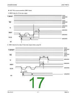
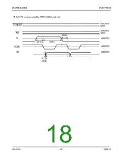
[ASAHI KASEI]
[AK7740ET]
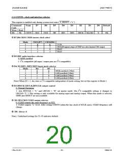
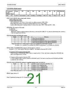
2-2) CONT1: RAM control
Command
Code
Name
D7
D6
D5
D4
D3
D2
D1
D0 Default
Write Read
64h
74h
CONT1 DATARAM
RM
BANK[1]
BANK[0] CMP_N
SS[1]
SS[0]
X
00h
c D7: DATARAM addressing mode selector
0:Ring addressing mode
1:Linear addressing mode
DATARAM has 256-word x 24-bit with two address pointers (DP0, DP1).
Ring addressing mode: increments starting address by one every sample.
Linear addressing mode: starting address is always the same: DP0 = 00h and DP1 = 80h.
d D6:RM: decompress bit mode
0: SIGN bit
1: Random data
When the compress and decompress function is selected (D3:CMP_N = 0), this bit determines the content o
f the decompressed LSB bits.
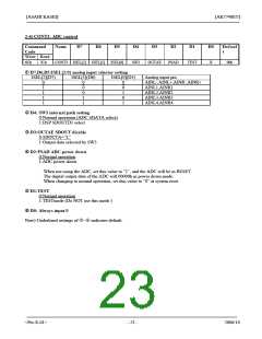
e D5,D4:BANK[1:0] DLRAM setting
Mode
D5
D4
0
Memory
0
1
2
3
0
24bit 3kword (RAM A)
12bit 6kword (RAM A)
0
1
1
0
1
12bit 4kword (RAM A),24bit 1kword (RAM B)
24bit 1kword (RAM A),12bit 4kword (RAM B)
1
Note) In mode 0 or 1, both pointer 0 and 1 are available for both RAM A and B.
In mode 2 or 3, pointer 0 is available for RAM A and pointer 1 is available for RAM B.
f D3:CMP_N 12bitDLRAM compress & decompress selector
In mode 1,2 or 3, this register turns the compress / decompress function ON or OFF.
0: Compress & decompress function ON
When writing to DLRAM the DBUS data is compressed to 12-bits, and when reading from DLRAM, the
data is decompressed to 16-bits.
1: Compress & decompress function OFF
12-bits of DBUS data is always written to DLRAM, and 12-bit data is read from the DLRAM and 000h
is added for the LSB bits.
g D2,D1:SS[1:0] DLRAM setting of sampling timing (only for RAM A)
Mode
D2
D1
RAM A mode selected by BANK[1:0]
0
1
2
3
0
0
Update every sampling time
0
1
Update every 2 sampling time
Update every 4 sampling time
Update every 8 sampling time
1
0
1
1
Note) When the mode 1,2 or 3 is selected, it comes out aliasing.
h D0: Input always 0
Note) Underlined settings for c~g indicates default.
<Pre-E-01>
- 21 -
2006/10

 AKM [ ASAHI KASEI MICROSYSTEMS ]