[ASAHI KASEI]
[AK7740ET]
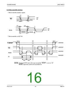
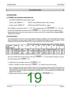
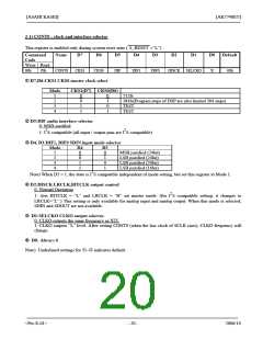
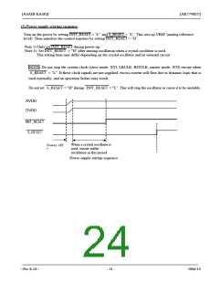
2-1) CONT0 : clock and interface selector
This register is enabled only during system reset state ( S_RESET =”L”).
Command
Code
Name
D7
D6
D5
D4
D3
D2
D1
D0
Default
Write Read
60h
70h
CONT0
CKS1
CKS0
DIF
DIF1
DIF0
DISCK SELCKO
X
00h
c D7,D6:CKS1 CKS0 master clock select
Mode
CKS1(D7) CKS0(D6)
1
2
3
4
0
0
1
1
0
1
0
1
512fs
384fs(Program steps of DSP are also limited 384 steps)
TEST
TEST
d D5:DIF audio interface selector
0: MSB-justified
1: I S compatible (all input / output pins are I S compatible)
2
2
e D4, D3:DIF1, DIF0 SDIN input mode selector
Mode
D4
0
D3
0
1
2
3
4
MSB justified (24bit)
LSB justified (24bit)
LSB justified (20bit)
LSB justified (16bit)
0
1
1
1
0
1
2
Note) When D5 = 1, the state is I S compatible independent of mode setting, but set this register to Mode 1.
f D2:DISCK LRCLK,BITCLK output control
0: Normal Operation
2
1: Sets BITCLK = ”L” and LRCLK = ”H” int master mode. (for I S compatible setting, it changes to
LRCLK=”L”.) This setting is only available for analog input and analog output. When this mode is selected,
SDIN and SDOUT are not available.
g D1:SELCKO CLKO output selector.
0: CLKO outputs the same frequency as XTI.
1: CLKO outputs “L” level. After setting CONT0 (when the last clock of SCLK rises), CLKO frequency will
change.
h D0: Always 0
Note) Underlined settings for c~g indicates default.
<Pre-E-01>
- 20 -
2006/10

 AKM [ ASAHI KASEI MICROSYSTEMS ]