[AK4679]
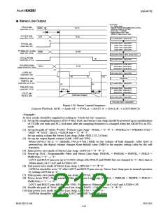
■ Receiver-Amp Output
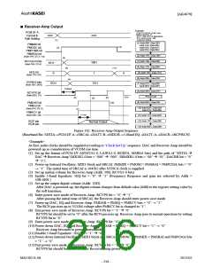
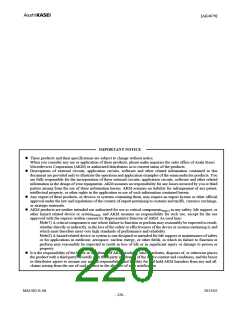
Example:
PCM I/F A
PCM I/F A Format : Linear, Long
MSBSA=BCKPA= “0”
xxxx
xxxx
Format &
DATT: −8dB, DATT-B: 0dB(default)
RCV Volume Level: −6dB
5 band EQ: Enable
Path Setting
(1)
(1) Addr:09H, Data:20H
Addr:14H, Data:40H
Addr:20H, Data:01H
Addr:25H, Data:00H
PMMIX bit
PMOSC bit
PMPCMA bit
(12)
(2)
PMSRAI bit
(2) Addr:1FH, Data:1BH
(3) Addr:10H, Data:90H
(4) Addr:17H, Data:0AH
(5) Addr:1EH, Data:1CH
(6) Addr:0DH, Data:02H
(Addr:1FH, D7,3, 1-0)
(3)
RCVG3-0 bits
(Addr:10H, D7-4)
1001
1011
0
(4)
(11)
5EQ bit
(Addr:17H, D3)
1
0
(5)
OVR6-0 bits
(Addr:1EH, D6-0)
0CH
1CH
(7) Addr:01H, Data:09H
Addr:0DH, Data:03H
156/fs2
(8) Addr:0DH, Data:01H
Phone Call
RCVPS bit
(Addr:0DH, D1)
(13)
(6)
(9)
(8)
(9) Addr:0DH, Data:03H
(10)
PMDAR bit
PMEQ bit
(Addr:01H, D3, 0)
(10) Addr:0DH, Data:02H
Addr:01H, Data:00H
(7)
PMRCV bit
>1 ms
(Addr:0DH, D0)
(11) Addr:17H, Data:02H
(12) Addr:1FH, Data:00H
(13) Addr:0DH, Data:00H
RCP pin
RCN pin
Normal Output
Figure 162. Receiver-Amp Output Sequence
(Baseband Rx: SDTIA→PCM I/F A→SRCAI→DATT-B→MIX1R→5-Band EQ→DATT-A→DACR→RCP/RCN)
<Example>
At first, audio clocks should be supplied according to “Clock Set Up” sequence. DAC and Receiver-Amp should be
powered-up in consideration of VCOM rise time
(1) Set up the format of PCM I/F A(FMTA1-0, LAWA1-0, BCKPA, MSBSA bits) and the path of “SDTIA Æ
DAC Æ Receiver-Amp”(MX1R2-0 bits = “000” Æ “000”, SRMXR1-0 bits = “00” Æ “01”, DACRR bit = “0”
Æ “1”)
(2) Power-up Internal Oscillator, MIX1 block and SRCAI: PMMIX = PMOSC= PMSRAI = PMPCMA bits = “0”
→ “1”. The initial time of SRCAI is 164/fs2 after SYNCA clock is supplied.
(3) Set up analog volume for Receiver-Amp (Addr: 10H, RCVG3-0 bits)
(4) Enable 5-band Equalizer: 5EQ bit = “0” Æ “1” (Frequency Response and gain are selected by Addr =
50H-6EH.)
(5) Set up the output digital volume (Addr: 1EH)
After DAC is powered-up, the digital volume changes from default value (0dB) to the register setting value by
the soft transition.
(6) Enter power-save mode of Receiver-Amp: RCVPS bit = “0” Æ “1”
After passing the initial time of SRCAI, the Receiver-Amp should enter power-save mode.
(7) Power-up DAC, EQ and Receiver-Amp: PMDAR = PMEQ = PMRCV bits = “0” → “1”
The RCN pin rises up to VCOM voltage after PMRCV bit is changed to “1”.
(8) Exit power-save mode of Receiver-Amp: RCVPS bit = “1” Æ “0”
RCVPS bit should be set to “0” after the RCN pin rises up. Receiver-Amp goes to normal operation by setting
RCVPS bit to “0”.
(9) Enter power-save mode of Receiver-Amp: RCVPS bit: “0” Æ “1”
(10)Power-down DAC, EQ and Receiver-Amp: PMDAR = PMEQ = PMRCV bit = “1” → “0”
Receiver-Amp becomes to power-down mode.
(11)Disable 5-band Equalizer: 5EQ bit = “1” Æ “0”
(12)Power-down Internal Oscillator, MIX1 block and SRCAI: PMOSC = PMMIX = PMSRAI and PMPCMA bits
= “1” → “0”
(13)Exit power-save mode of Receiver-Amp: RCVPS bit = “1” Æ “0”
RCVPS bit should be set to “0” after Receiver-Amp power-down.
MS1402-E-06
2013/02
- 216 -

 AKM [ ASAHI KASEI MICROSYSTEMS ]