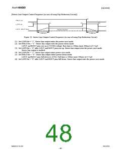
[AK4646]
■ Serial Control Interface
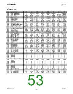
Internal registers may be written by using the 3-wire µP interface pins (CSN, CCLK and CDTIO). The data on this
interface consists of Read/Write, Register address (MSB first, 7bits) and Control data (MSB first, 8bits). Each bit is
clocked in on the rising edge (“↑”) of CCLK. It is available for writing data on the rising edge of CSN. When reading
operation, CDTIO pin has become an output mode at the falling edge of 8th CCLIC and outputs D7-D0. The output
finishes on the rising edge of CSN. The CDTIO is placed in a Hi-Z state except outputting data at read operation mode.
Clock speed of CCLK is 5MHz (max). The value of internal registers are initialized by PDN pin = “L”.
Note 41. It is available for reading the address 00H~11H. When reading the address 12H ∼ 7FH, the register values are
invalid.
CSN
0
2
6
7
8
9
10 11
12 13 14 15
1
3
4
5
CCLK
“H” or “L”
“H” or “L”
“H” or “L”
R/W
A6 A5
A4 A3 A2 A1 A0 D7 D6 D5 D4 D3 D2 D1 D0
CDTIO “H” or “L”
R/W:
READ/WRITE (“1”: WRITE, “0”: READ)
A6-A0: Register Address
D7-D0: Control data (Input) at Write Command
Output data (Output) at Read Command
Figure 36. Serial Control I/F Timing
MS0557-E-05
2011/01
- 52 -

 AKM [ ASAHI KASEI MICROSYSTEMS ]