ASAHI KASEI
[AK4522]
OPERATION OVERVIEW
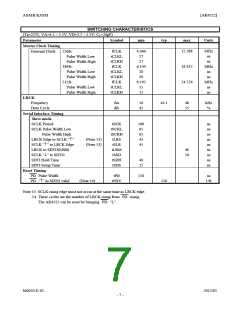
System Clock
The master clock (MCLK) can be external clock input to the MCKI pin. CMODE is used to select either MCLK=256fs,
384fs or 512fs. The relationship between the MCLK and the desired sample rate is defined in Table 1. The LRCK clock
input must be synchronized with MCLK, however the phase is not critical. Internal timing is synchronized to LRCK upon
power-up. All external clocks must be present unless PD = “L”, otherwise excessive current may result from abnormal
operation of internal dynamic logic.
MCLK
384fs
CMODE=”H”
12.2880MHz
16.9344MHz
18.4320MHz
SCLK
fs
256fs
CMODE=”L”
8.1920MHz
11.2896MHz
12.2880MHz
512fs
CMODE=”NC”
64fs
128fs
32.0kHz
44.1kHz
48.0kHz
16.384MHz
22.579MHz
24.576MHz
2.048MHz
2.822MHz
3.072MHz
4.096MHz
5.644MHz
6.144MHz
Table 1. System Clock Example
Audio Serial Interface Format
Data is shifted in/out the SDTI/SDTO pins using SCLK and LRCK inputs. Four serial data modes selected by the DIF0
and DIF1 pins are supported as shown in Table 2. In all modes the serial data has MSB first, 2’s compliment format. The
data is clocked out on the falling edge of SCLK and latched on the rising edge. For mode 3, if SCLK is 32fs, then the least
significant bits will be truncated.
Mode
DIF1
DIF0
SDTO (ADC)
20bit, MSB justified
20bit, MSB justified
20bit, MSB justified
IIS (I2S)
SDTI (DAC)
16bit, LSB justified
20bit, LSB justified
20bit, MSB justified
IIS (I2S)
L/R
H/L
H/L
H/L
L/H
SCLK
≥ 32fs
≥ 40fs
0
1
2
3
0
0
1
1
0
1
0
1
≥ 40fs
≥ 32fs or 40fs
Table 2. Serial Data Modes
LRCK(i)
0
1
2
3
9
10
11
12
13
14
15
0
1
2
9
10
11
12
13 14
15
0
1
SCLK(i:32fs)
SDTO(o)
19 18 17
15 14 13
11 10
9
5
8
4
7
3
6
2
5
1
4
0
19 18 17
15 14 13
11 10
9
8
7
3
6
2
5
1
4
0
19
15
7
6
7
6
5
4
SDTI(i)
0
1
2
3
17
18
19 20
30
31
0
1
2
3
17
18
19
20
31
0
1
SCLK(i:64fs)
SDTO(o)
19 18 17
3
2
1
0
19 18 17
3
2
1
0
19
15 14 13 12 11
2
1
0
15 14 13 12 11
Rch Data
2
1
0
Don’t Care
Don’t Care
SDTI(i)
SDTO-19:MSB, 0:LSB; SDTI-15:MSB, 0:LSB
Lch Data
Figure 1. Mode 0 Timing
M0020-E-02
2012/01
- 9 -

 AKM [ ASAHI KASEI MICROSYSTEMS ]