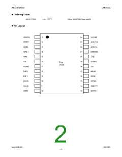
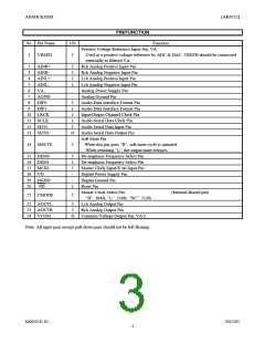
ASAHI KASEI
[AK4522]
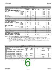
FILTER CHARACTERISTICS
(Ta=25°C; VA=4.5 ∼ 5.5V, VD=2.7 ∼ 5.5V; fs=44.1kHz; DEM0=”1”, DEM1=”0”)
Parameter
Symbol
min
typ
max
Units
ADC Digital Filter (Decimation LPF):
Passband
(Note 10) -0.005dB
PB
0
0
0
19.76
20.02
20.20
22.05
kHz
kHz
kHz
kHz
kHz
dB
dB
1/fs
us
-0.02dB
-0.06dB
-6.0dB
0
Stopband
SB
PR
SA
GD
ΔGD
24.34
Passband Ripple
Stopband Attenuation
Group Delay
±0.005
80
(Note 11)
29.3
0
Group Delay Distortion
ADC Digital Filter (HPF):
Frequency Response
(Note 10) -3dB
FR
0.9
2.7
6.0
Hz
Hz
Hz
-0.5dB
-0.1dB
DAC Digital Filter:
Passband
(Note 10) -0.06dB
-6.0dB
PB
0
0
24.1
20.0
22.05
kHz
kHz
kHz
dB
dB
1/fs
Stopband
SB
PR
SA
GD
Passband Ripple
Stopband Attenuation
Group Delay
±0.06
43
(Note 11)
14.7
DAC Digital Filter + Analog Filter:
Frequency Response: 0 ∼ 20.0kHz
FR
dB
±0.2
Note:10. The passband and stopband frequencies scale with fs.
For example, 20.02kHz at -0.02dB is 0.454 x fs. The reference frequency of these responses is 1kHz.
11. The calculating delay time which occurred by digital filtering. This time is from the input of analog signal to
setting the 20bit data of both channels to the output register for ADC.
For DAC, this time is from setting the 20bit data of both channels on input register to the output of analog
signal.
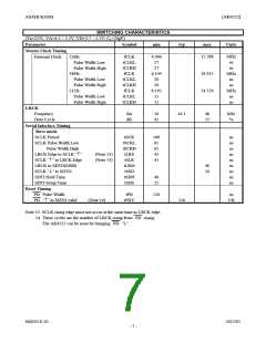
DIGITAL CHARACTERISTICS
(Ta=25°C; VA=4.5 ∼ 5.5V, VD=2.7 ∼ 5.5V)
Parameter
Symbol
VIH
VIL
min
70%VD
-
typ
-
-
Max
-
30%VD
Units
V
V
High-Level Input Voltage (Except CMODE
pin)
Low-Level Input Voltage (Except CMODE
pin)
High-Level Input Voltage (CMODE pin)
Low-Level Input Voltage (CMODE pin)
VIH
VIL
VOH
VOL
Iin
95%VD
-
-
-
-
-
-
10%VD
-
0.4
±10
V
V
V
V
uA
-
Hight-Level Output Voltage
Low-Level Output Voltage
Input Leakage Current
(Iout=-80uA)
(Iout=80uA)
(Note 12)
VD-0.4
-
-
Note: 12. CMODE pin has internal pull-up and pull-down devices, nominally 50kohm.
M0020-E-02
2012/01
- 6 -

 AKM [ ASAHI KASEI MICROSYSTEMS ]