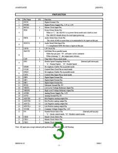
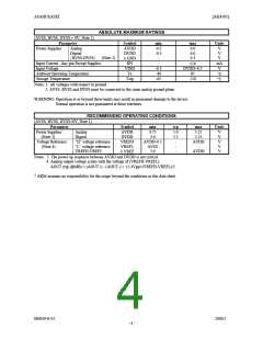
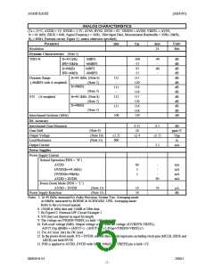
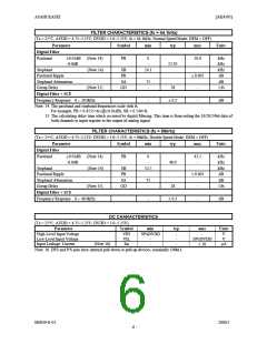
ASAHI KASEI
[AK4393]
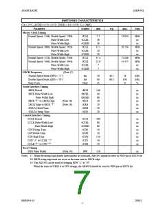
SWITCHING CHARACTERISTICS
(Ta = 25°C; AVDD = 4.75~5.25V; DVDD = 3.0~5.25V; CL = 20pF)
Parameter
Symbol
min
typ
max
Units
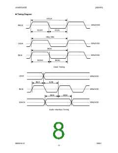
Master Clock Timing
Normal Speed: 256fs, Double Speed: 128fs
Pulse Width Low
fCLK
tCLKL
tCLKH
fCLK
7.7
28
13.824
MHz
ns
Pulse Width High
28
ns
Normal Speed: 384fs, Double Speed: 192fs
Pulse Width Low
11.5
20
20.736
MHz
ns
tCLKL
tCLKH
fCLK
Pulse Width High
20
ns
Normal Speed: 512fs, Double Speed: 256fs
Normal Speed: 768fs, Double Speed: 384fs
Pulse Width Low
15.4
23.0
7
27.648
41.472
MHz
MHz
ns
fCLK
tCLKL
tCLKH
Pulse Width High
7
ns
LRCK Frequency
Normal Speed Mode (DFS = “L”)
(Note 17)
fsn
fsd
30
60
45
44.1
88.2
54
108
55
kHz
kHz
%
Double Speed Mode (DFS = “H”)
Duty Cycle
Duty
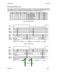
Serial Interface Timing
BICK Period
tBCK
tBCKL
tBCKH
tBLR
140
60
60
20
20
20
20
ns
ns
ns
ns
ns
ns
ns
BICK Pulse Width Low
Pulse Width High
BICK “” to LRCK Edge
LRCK Edge to BICK “”
SDATA Hold Time
SDATA Setup Time
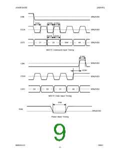
Control Interface Timing
CCLK Period
(Note 18)
(Note 18)
tLRB
tSDH
tSDS
tCCK
tCCKL
tCCKH
tCDS
200
80
ns
ns
ns
ns
ns
ns
ns
ns
CCLK Pulse Width Low
Pulse Width High
80
CDTI Setup Time
50
CDTI Hold Time
tCDH
tCSW
tCSS
50
CSN High Time
150
50
CSN “¯” to CCLK “”
CCLK “” to CSN “”
Reset Timing
tCSH
50
PDN Pulse Width
(Note 19)
tPW
150
ns
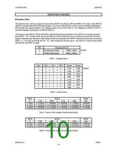
Notes: 17. When the normal and double speed modes are switched, AK4393 should be reset by PDN pin or RSTN bit.
18. BICK rising edge must not occur at the same time as LRCK edge.
19. The AK4393 can be reset by bringing PDN “L” to “H”.
When the states of CKS2-0 or DFS change, the AK4393 should be reset by PDN pin or RSTN bit.
M0039-E-01
2000/5
- 7 -

 AKM [ ASAHI KASEI MICROSYSTEMS ]