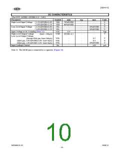
[AK4372]
Parameter
Symbol
min
typ
max
Units
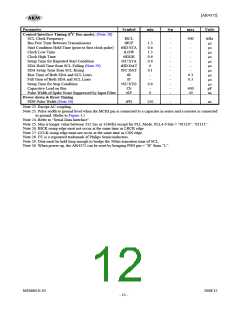
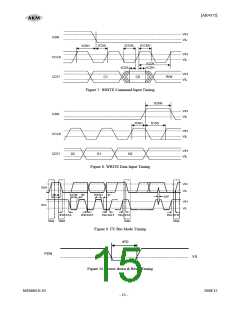
Control Interface Timing (I2C Bus mode): (Note 28)
SCL Clock Frequency
fSCL
tBUF
-
-
-
-
-
-
-
-
-
-
-
-
-
-
400
-
-
-
-
-
-
-
0.3
0.3
-
400
50
kHz
μs
μs
μs
μs
μs
μs
μs
μs
μs
μs
pF
ns
Bus Free Time Between Transmissions
Start Condition Hold Time (prior to first clock pulse)
Clock Low Time
1.3
0.6
1.3
0.6
0.6
0
0.1
-
-
tHD:STA
tLOW
tHIGH
tSU:STA
tHD:DAT
tSU:DAT
tR
Clock High Time
Setup Time for Repeated Start Condition
SDA Hold Time from SCL Falling (Note 29)
SDA Setup Time from SCL Rising
Rise Time of Both SDA and SCL Lines
Fall Time of Both SDA and SCL Lines
Setup Time for Stop Condition
tF
tSU:STO
Cb
0.6
-
0
Capacitive Load on Bus
Pulse Width of Spike Noise Suppressed by Input Filter
tSP
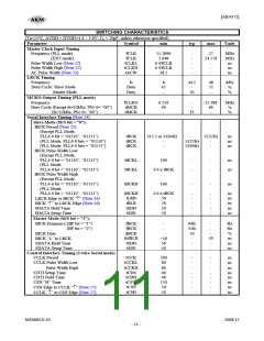
Power-down & Reset Timing
PDN Pulse Width (Note 30)
tPD
150
-
-
ns
Note 22. Except AC coupling.
Note 23. Pulse width to ground level when the MCKI pin is connected to a capacitor in series and a resistor is connected
to ground. (Refer to Figure 3.)
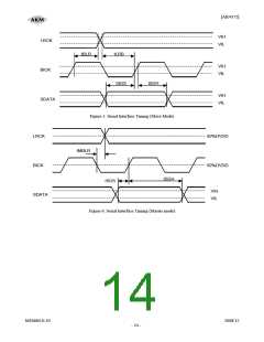
Note 24. Refer to “Serial Data Interface”.
Note 25. Min is longer value between 312.5ns or 1/(64fs) except for PLL Mode, PLL4-0 bits = “01110”, “01111”.
Note 26. BICK rising edge must not occur at the same time as LRCK edge.
Note 27. CCLK rising edge must not occur at the same time as CSN edge.
Note 28. I2C is a registered trademark of Philips Semiconductors.
Note 29. Data must be held long enough to bridge the 300ns-transition time of SCL.
Note 30. When power-up, the AK4372 can be reset by bringing PDN pin = “H” from “L”.
MS0684-E-02
2008/12
- 12 -

 AKM [ ASAHI KASEI MICROSYSTEMS ]