PDF
最近搜索
热门搜索
发布采购

| 型号: | AK4252 |
| PDF下载: | 下载PDF文件 查看货源 |
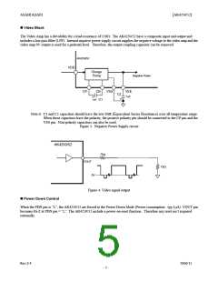
| 内容描述: | 输出耦合电容的视频放大器,低通滤波器 [Output Coupling Capacitor-less Video Amp with LPF] |
| 分类和应用: | 视频放大器 |
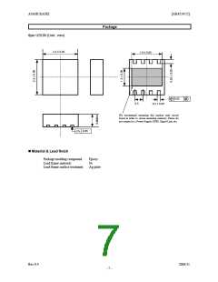
| 文件页数/大小: | 9 页 / 72 K |
| 品牌: |  AKM [ ASAHI KASEI MICROSYSTEMS ] AKM [ ASAHI KASEI MICROSYSTEMS ] |
专业IC领域供求交易平台:提供全面的IC Datasheet资料和资讯,Datasheet 1000万数据,IC品牌1000多家。