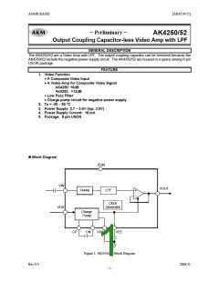
ASAHI KASEI
No. Pin Name
[AK4250/52]
PIN/FUNCTION
I/O
O
-
Function
Positive Charge Pump Capacitor Terminal Pin
CP
1
2
3
VDD
VIN
Power Supply Pin.
I
Composite Video Signal Input Pin
Power-Down Mode Pin. Internal Pull Down 100kΩ.
“H”: Power up, “L”: Power down.
Composite Video Signal Driver Pin
4
PDN
I
5
6
7
8
VOUT
VSS
VEE
CN
O
-
Ground Pin
Negative Voltage Output Pin for Video Amplifier
Negative Charge Pump Capacitor Terminal Pin
O
I
ABSOLUTE MAXIMUM RATINGS
(VSS=0V; Note1)
Parameter
Symbol
VDD
IIN
min
−0.3
-
max
Units
V
Power Supplies:
4.0
Input Current, Any Pin Except Supplies
Input Voltage (Note 2)
±10
mA
V
VIN
Ta
Tstg
−0.3
−40
−65
(VDD+0.3) or 4.0
Ambient Temperature (powered applied)
Storage Temperature
85
150
°C
°C
Note 1. All voltages with respect to ground.
Note 2. VIN, PDIN pins. Max is smaller value between (VDD+0.3)V and 4.0V
VOUT pin becomes Hi-Z at PDN pin = “L”. Therefore VOUT pin is available to signal line from another device
by Wired-OR. Then the input signal to VOUT pin mustn’t exceeds this input voltage range.
The voltage must not be applied to the CN pin.
WARNING: Operation at or beyond these limits may result in permanent damage to the device.
Normal operation is not guaranteed at these extremes.
RECOMMENDED OPERATING CONDITIONS
(VSS=0V; Note1)
Parameter
Symbol
min
typ
max
Units
Power Supplies
VDD
2.7
3.0
3.6
V
Note 1. All voltages with respect to ground.
* AKM assumes no responsibility for the usage beyond the conditions in this datasheet.
Rev.0.4
2006/11
- 3 -

 AKM [ ASAHI KASEI MICROSYSTEMS ]