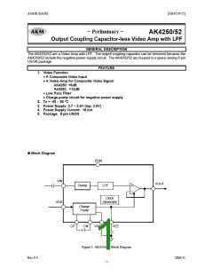
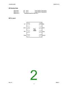
ASAHI KASEI
[AK4250/52]
ANALOG CHRACTERISTICS
(Ta=25°C; VDD =3.0V; VSS = 0V; unless otherwise specified)
Parameter
Conditions
Min
typ
max
Units
V Input Characteristics
Input Voltage
AK4250
AK4252
AK4250
AK4252
-
-
-
-
1.5
0.75
Vpp
Vpp
V
V
Input Sync Chip Clamp
Voltage
(Note 3)
-0.386 -0.286 -0.186
TBD
-0.143
TBD
V Output Characteristics (Note 4)
Output Gain
VIN=100kHz, 0.2Vpp
VIN=100kHz, TBD Vpp
VIN=100kHz , THD=-30dB
AK4250
AK4252
AK4250
AK4252
AK4250
AK4252
5.0
TBD
2.52
2.52
-
-
-
140
-
6.0
12.0
-
7.0
TBD
-
-
-
-
-
-
dB
dB
Vpp
Vpp
dB
dB
dB
Ω
Maximum output voltage
S/N
-
65
62
-45
150
-
BW=100kH ∼ 6MHz, (Note 5)
Secondary Distortion
Load Resistance
Load Capacitance
VIN=3.58MHz, 0.2Vpp(Sin Wave)
C1(see Figure 2)
C2(see Figure 2)
15
400
pF
pF
-
-
LPF
Frequency Response
Input= 0.2Vpp, Sin Wave
(0dB at 100kHz)
Group Delay
Response at 6.75MHz
Response at 27MHz
TBD
-
-0.5
-40
-
dB
dB
TBD
|GD3MHz - GD6MHz|
-
10
TBD
nsec
Power Supplies
Power Up
Power Down
Black signal is output and no load resistance.
PDN pin = 0V
-
-
10
1
TBD
TBD
mA
μA
Note 3. The Charge Pump circuit doesn’t work well, if the sync chip clamp voltage input to VIN pin isn’t within this voltage
range. This sync chip clamp voltage is the voltage from the pedestal voltage
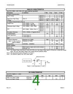
Note 4. The measurement point is the point A in Figure 2
Note 5. The reference signal is the 100% white signal.
Measurement Point A
75 ohm
Video Signal Output
R2
R1
75 ohm
C1
C2
Figure 2. Load Capacitance C1 and C2
DC CHRACTERISTICS
(Ta=25°C; VDD=2.7 ∼ 3.6V)
Parameter
Symbol
VIH
VIL
min
1.5
-
typ
max
-
0.6
Units
V
V
High-Level Input Voltage
Low-Level Input Voltage
(PDN pin)
(PDN pin)
-
-
Rev.0.4
2006/11
- 4 -

 AKM [ ASAHI KASEI MICROSYSTEMS ]