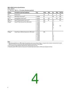
MGA-62563 Electrical Specifications
Rbias=240ohm
TC = 25°C, ZO = 50Ω, Vd = 3V (unless otherwise specified)
Symbol
Parameters and Test Conditions
Freq
Units
Min.
Typ.
Max. Std Dev
Id[1,2]
Device Current
mA
dB
47
62
77
2.09
0.06
0.36
0.51
[1,2]
NFtest
Noise Figure in test circuit[1]
f = 0.5 GHz
f = 0.5 GHz
f = 0.5 GHz
0.93
22
1.4
23.4
[1,2]
Gtest
Associated Gain in test circuit[1]
Ouput 3rd Order Intercept in test circuit[1]
Output 3rd Order Intercept Point in 50Ω system
dB
20.4
30
[1,2]
OIP3test
OIP350Ω
dBm
dBm
32.9
[3]
f = 0.1 GHz
f = 0.2 GHz
f = 0.5 GHz
f = 1.0 GHz
f = 1.5 GHz
f = 2.0 GHz
f = 2.5 GHz
f = 3.0 GHz
34.7
34.7
34.8
33.5
33
32.3
32
31
0.51
[3]
P1dB50Ω
Output Power at 1dB Gain Compression in 50Ω system
f = 0.1 GHz
f = 0.2 GHz
f =0.5 GHz
f = 1.0 GHz
f = 1.5 GHz
f = 2.0 GHz
f = 2.5 GHz
f = 3.0 GHz
dBm
18
18
18
17.6
17.6
17.7
17.9
17.7
Notes:
1. Guaranteed specifications are 100% tested in the production test circuit as shown in Figure 1, the typical value is based on measurement of at least
500 parts from three non-consecutive wafer lots during initial characterization of this product.
2. Circuit achieved a trade-off between optimal NF, Gain, OIP3 and input return loss.
3. Parameter quoted at 50Ω is based on measurement of selected typical parts tested on a 50Ω input and output test fixture.
4

 AGILENT [ AGILENT TECHNOLOGIES, LTD. ]