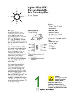
Simplified Schematic
Vd
Ibias
Id = Ids + Ibias
Rbias
Ids
Feedback
Vbias
4
Input
match
3
6
Bias
1, 2, 5
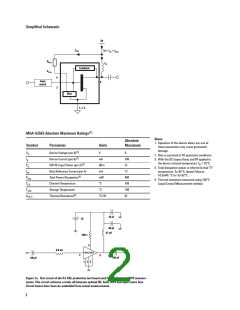
MGA-62563 Absolute Maximum Ratings[1]
Notes:
Absolute
1. Operation of this device above any one of
these parameters may cause permanent
damage.
Symbol
Parameter
Units
Maximum
Vd
Device Voltage (pin 6)[2]
Device Current (pin 6)[2]
CW RF Input Power (pin 3)[3]
Bias Reference Current (pin 4)
Total Power Dissipation[4]
Channel Temperature
V
6
2. Bias is assumed at DC quiescent conditions.
Id
mA
dBm
mA
mW
°C
100
21
3. With the DC (typical bias) and RF applied to
the device at board temperature TB = 25°C.
Pin
4. Total dissipation power is referred to lead "5"
temperature. Tc=92°C, derate Pdiss at
10.3mW/°C for Tc>92°C.
Iref
12
Pdiss
TCH
TSTG
θch_b
600
150
150
97
5. Thermal resistance measured using 150°C
Liquid Crystal Measurement method.
Storage Temperature
°C
Thermal Resistance[5]
°C/W
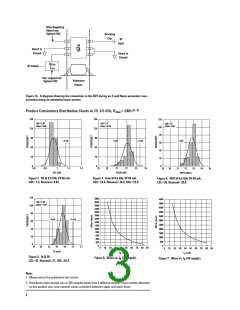
+
10 nF
68 pF
3V
47 nH
240Ω
4
6.8 nH
MGA-62563
3
6
100 pF
100 pF
1
2 5
Figure 1a. Test circuit of the 0.5 GHz production test board used for NF, Gain and OIP3 measure-
ments. This circuit achieves a trade-off between optimal NF, Gain, OIP3 and input return loss.
Circuit losses have been de-embedded from actual measurements.
2

 AGILENT [ AGILENT TECHNOLOGIES, LTD. ]