reflection coefficient greater than
unity) at the input of the MMIC.
These stability effects are entirely
predictable. A circuit simulation
using the data sheet S-parameters
Emitter Inductance and
Performance
As a direct result of their circuit
topology, the performance of INA
MMICs is extremely sensitive to
groundpath (“emitter”) induc-
tance. The two stage design
creates the possibility of a feed-
back loop being formed through
the ground returns of the stages. If
the path to ground provided by
the external circuit is “long” (high
in impedance) compared to the
path back through the ground
return of the other stage, then
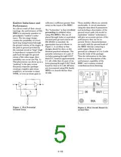
instability can occur (see Fig. 1).
This phenomena can show up as a
“peaking” in the gain versus
The “bottomline” is that excellent and including a description of the
grounding is critical when
using INA MMICs. The use of
plated through holes or equivalent will give an accurate picture of the
minimal path ground returns at
the device is essential. An
appropriate layout is shown in
Figure 2. A corollary is that
designs should be done on the
thinnest practical substrate. The
parasitic inductance of a pair of
via holes passing through 0.032"
thick P.C. board is approximately
0.1 nH, while that of a pair of via
ground return path (via model or
equivalent “emitter” inductance)
performance that can be ex-
pected. Device characterizations
are made with the ground leads of
the MMIC directly contacting a
solid copper block (system
ground) at a distance of 2 to 4 mils
from the body of the package.
Thus the information in the data
sheet is a true description of the
performance capability of the
holes passing through 0.062" thick MMIC, and contains minimal
board is close to 0.5 nH. HP does
not recommend using INA family
MMICs on boards thicker than
32 mils.
contributions from fixturing.
frequency response (perhaps
creating a negative gain slope
amplifier), an increase in input
VSWR, or even as return gain (a
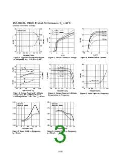
Figure 1. INA Potential
Ground Loop.
Figure 2. INA Circuit Board 2x
Actual Size.
6-100

 AGILENT [ AGILENT TECHNOLOGIES, LTD. ]