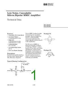
INA-02184, -02186 Absolute Maximum Ratings
Parameter
AbsoluteMaximum[1]
Thermal Resistance[2]:
θjc =90°C/W—INA-02184
θjc = 100°C/W — INA-02186
Device Current
PowerDissipation[2,3,4]
RF Input Power
Junction Temperature
Storage Temperature
50 mA
400mW
+13dBm
+150°C
Notes:
1. Permanent damage may occur if
any of these limits are exceeded.
2. TCASE=25°C.
–65to150°C
3. Derate at 11.1 mW/°C for TC >
144°CforINA-02184.
4. Derate at 10 mW/°C for TC > 110°C
forINA-02186.
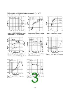
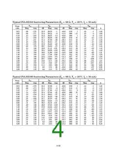
INA-02184, -02186 Electrical Specifications[1], TA = 25°C
INA-02184
INA-02186
Symbol Parameters and Test Conditions: Id = 35 mA, ZO = 50 Ω Units Min. Typ. Max. Min. Typ. Max.
GP
PowerGain(|S21|2)
f=0.5GHz
dB
29.0 31.0
± 2.0
0.8
29.0 31.0
± 2.0
0.8
∆GP
f3 dB
ISO
Gain Flatness
3 dB Bandwidth[2]
ReverseIsolation(|S12|2)
Input VSWR (Max over Freq. Range)
Output VSWR (Max over Freq. Range)
50 Ω Noise Figure
f=0.01to1.0GHz dB
GHz
f=0.01to1.0GHz dB
f=0.01to1.0GHz
f=0.01to1.0GHz
39
39
1.5
2.0
VSWR
1.7
1.7
NF
f=0.5GHz
f=0.5GHz
f=0.5GHz
f=0.5GHz
dB
dBm
dBm
psec
V
2.0
2.0
P1 dB
IP3
Output Power at 1 dB Gain Compression
Third Order Intercept Point
Group Delay
11
11
23
23
tD
330
350
Vd
Device Voltage
4.0 5.5
+10
7.0
4.0 5.5
+10
7.0
dV/dT
Device Voltage Temperature Coefficient
mV/°C
Notes:
1. The recommended operating current range for this device is 30 to 40 mA. Typical performance as a function of current
is on the following page.
2. Referenced from 10 MHz Gain (GP).
INA-02184, -02186 Part Number Ordering Information
Part Number
No. of Devices
Container
INA-02184-TR1
INA-02184-BLK
1000
100
7" Reel
Antistatic Bag
INA-02186-TR1
INA-02186-BLK
1000
100
7" Reel
Antistatic Bag
For more information, see “Tape and Reel Packaging for Semiconductor Devices”.
6-97

 AGILENT [ AGILENT TECHNOLOGIES, LTD. ]