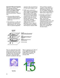
Appendix B: PCB Layout Suggestion
capacitors; they may be left out
if a clean power supply is used.
CX2 and CX3 are tantalum
capacitors of big volume and
fast frequency response. The
use of a tantalum capacitor is
more critical on the VLED line,
which carries a high current.
The following PCB layout
guidelines should be followed to
obtain a good PSRR and EM
immunity resulting in good
electrical performance. Things to
note:
3. VLED can be connected to
either unfiltered or unregulated
power supply. If VLED and Vcc
share the same power supply,
CX3 need not be used and the
connections for CX1 and CX2
should be before the current
limiting resistor R1. In a noisy
environment, including
4. Preferably a multi-layered
board should be used to
provide sufficient ground
plane. Use the layer
1. The ground plane should be
continuous under the part, but
should not extend under the
shield trace.
underneath and near the
transceiver module as Vcc, and
sandwich that layer between
ground connected board
layers. Refer to the diagram
below for an example of a
four-layer board.
capacitor CX2 can enhance
supply rejection. CX1 is
generally a ceramic capacitor
of low inductance providing a
wide frequency response while
2. The shield trace is a wide, low
inductance trace back to the
system ground. CX1, CX2 and
CX3 are optional supply filter
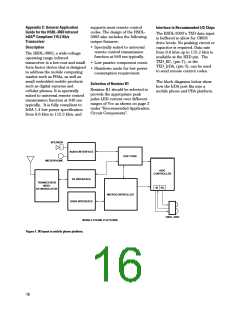
TOP LAYER
CONNECT THE METAL SHIELD AND MODULE
GROUND PIN TO BOTTOM GROUND LAYER.
LAYER 2
CRITICAL GROUND PLANE ZONE. DO NOT
CONNECT DIRECTLY TO THE MODULE
GROUND PIN.
LAYER 3
KEEP DATA BUS AWAY FROM CRITICAL
GROUND PLANE ZONE.
BOTTOM LAYER (GND)
The area underneath the module
at the second layer, and 3 cm in
all directions around the module,
is defined as the critical ground
plane zone. The ground plane
should be maximized in this zone.
Refer to application note AN1114
or the Agilent IrDA Data Link
Design Guide for details. The
layout below is based on a
two-layer PCB.
Top View
Bottom View
15

 AGILENT [ AGILENT TECHNOLOGIES, LTD. ]