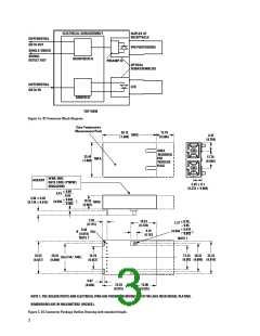
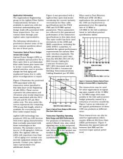
Transmitter Sections
The package outline drawings
and pin out are shown in
Figures 2, 2a and 3. The details
of this package outline and pin
out are compliant with the
The outer housing including the
duplex SC connector receptacle
or the duplex ST ports is molded
of filled nonconductive plastic to
provide mechanical strength and
electrical isolation. The solder
posts of the Agilent design are
isolated from the circuit design
of the transceiver and do not
The transmitter section of the
HFBR-5803 and HFBR-5805
series utilize 1300 nm Surface
Emitting InGaAsP LEDs. These
LEDs are packaged in the optical multisource definition of the 1 x
subassembly portion of the
transmitter section. They are
driven by a custom silicon IC
which converts differential
PECL logic signals, ECL
referenced (shifted) to a +3.3 V
or +5 V supply, into an analog
LED drive current.
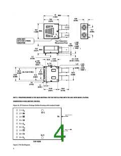
9 SIP. The low profile of the
Agilent transceiver design
complies with the maximum
height allowed for the duplex SC require connection to a ground
connector over the entire length
of the package.
plane on the circuit board.
The transceiver is attached to a
The optical subassemblies utilize printed circuit board with the
a high volume assembly process
together with low cost lens
elements which result in a cost
effective building block.
nine signal pins and the two
solder posts which exit the
bottom of the housing. The two
solder posts provide the primary
mechanical strength to
withstand the loads imposed on
the transceiver by mating with
duplex or simplex SC or ST
connectored fiber cables.
Receiver Sections
The receiver sections of the
HFBR-5803 and HFBR-5805
series utilize InGaAs PIN photo-
diodes coupled to a custom
silicon transimpedance
preamplifier IC. These are
packaged in the optical sub-
assembly portion of the receiver.
The electrical subassembly con-
sists of a high volume multilayer
printed circuit board on which
the IC chips and various surface-
mounted passive circuit
elements are attached.
These PIN/preamplifier combi-
nations are coupled to a custom
quantizer IC which provides the
final pulse shaping for the logic
output and the Signal Detect
function. The data output is dif-
ferential. The signal detect
The package includes internal
shields for the electrical and
optical subassemblies to ensure
low EMI emissions and high
immunity to external EMI fields.
output is single-ended. Both
data and signal detect outputs
are PECL compatible, ECL
referenced (shifted) to a +3.3 V
or +5 V power supply.
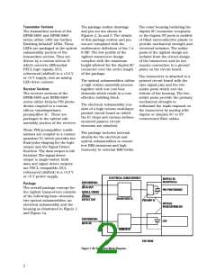
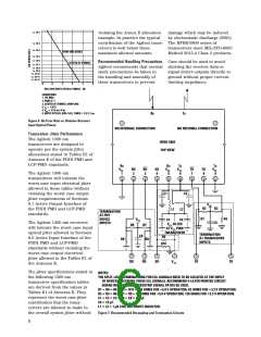
ELECTRICAL SUBASSEMBLY
DUPLEX SC
RECEPTACLE
DIFFERENTIAL
DATA OUT
Package
The overall package concept for
the Agilent transceivers consists
of the following basic elements;
two optical subassemblies, an
electrical subassembly and the
housing as illustrated in Figure 1
and Figure 1a.
PIN PHOTODIODE
SINGLE-ENDED
SIGNAL
QUANTIZER IC
DETECT OUT
PREAMP IC
OPTICAL
SUBASSEMBLIES
DIFFERENTIAL
DATA IN
LED
DRIVER IC
TOP VIEW
Figure 1. SC Connector Block Diagram.
2

 AGILENT [ AGILENT TECHNOLOGIES, LTD. ]