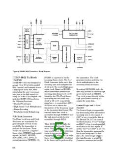
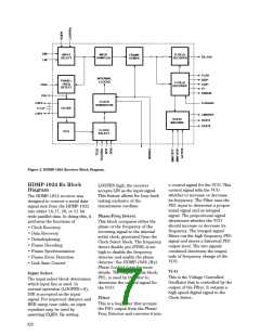
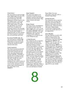
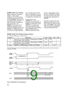
HDMP-1022 (Tx) Timing
Figure 6 shows the Tx timing
diagram. Under normal
rate. The data must be valid
before it’s sampled for a set-up
time (ts), and remain valid after
it’s sampled for a hold time (th).
reference with a delay of ∆Tstrb.
The rate of STRBOUT is always
the same as the word rate of the
incoming data, independent of
MDFSEL.
operations, the Tx PLL locks an
internally generated clock to the
incoming STRBIN. The incoming
data, D0-D19, ED, FF, DAV*,
CAV*, and FLAG, are latched by
this internal clock. For
MDFSEL=0, the input rate of
STRBIN is expected to be the
same as the parallel data rate. For
MDFSEL=1, STRBIN should be
1/2 of the incoming parallel data
In single frame mode
(MDFSEL=0), ts and th are
referenced to the rising edge of
STRBIN. In double frame mode
(MDFSEL=1), ts and th are
referenced to half the frame
period from the rising or falling
edge of STRBIN plus 4 ns.
STRBOUT appears after this
The start of a frame, D0, in the
high speed serial output occurs
after a delay of td after the rising
edge of the STRBIN. The typical
value of td may be calculated by
using the following formula.
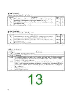
HDMP-1022 (Tx) Timing Characteristics
Tc = 0°C to +85°C, VCC = 4.5 V to 5.5 V
Symbol
Parameter
Units
Min. Typ. Max.
ts
Setup Time, for D0-D19 Relative to Rising Edge of STRBIN,
ED, FF, DAV*, CAV* and FLAG
nsec
2.0*
th
Hold Time, for D0-D19 Relative to Rising Edge of STRBIN,
ED, FF, DAV*, CAV* and FLAG
STRBOUT - STRBIN Delay at 64 MHz in 20-bit Mode
nsec
nsec
2.0*
∆Tstrb
4.0
*In double frame mode, due to the internal clock delay, ts and th are referenced to half the frame period plus 4 ns from the rising or
falling edge of STRBIN.
STRBIN
MDFSEL = 0
1/2 FRAME PERIOD
STRBIN
MDFSEL = 1
D00 - D19
ED, FF
DAV*, CAV*
FLAG
t
t
h
s
STRBOUT
DOUT
t
strb
D-FIELD
C-FIELD
t
d
HCLK
Figure 6. HDMP-1022 (Tx) Timing Diagram.
624

 AGILENT [ AGILENT TECHNOLOGIES, LTD. ]