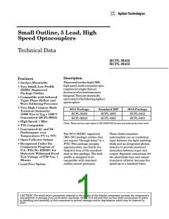
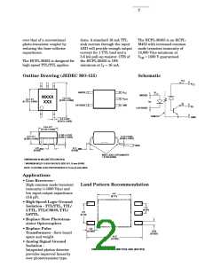
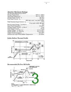
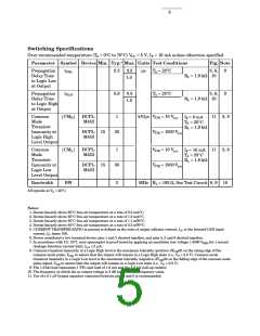
5
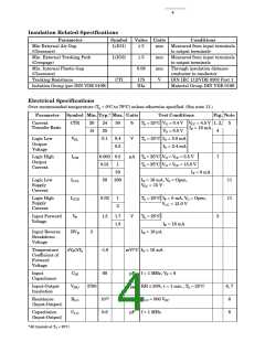
Switching Specifications
Over recommended temperature (TA = 0°C to 70°C) VCC = 5 V, IF = 16 mA unless otherwise specified.
Parameter Symbol Device Min. Typ.* Max. Units Test Conditions Fig. Note
Propagation
Delay Time
to Logic Low
at Output
tPHL
0.2
0.6
0.8
1.0
µs
TA = 25°C
TA = 25°C
5, 6,
RL = 1.9 kΩ 10
9
9
Propagation
Delay Time
to Logic High
at Output
tPLH
0.8
1.0
5, 6,
RL = 1.9 kΩ 10
Common
Mode
Transient
Immunity at
Logic High
Level Output
|CMH| HCPL-
M452
1
kV/µs VCM = 10 Vp-p
11 8, 9
IF = 0 mA
TA = 25°C
RL = 1.9 kΩ
HCPL- 15
M453
30
VCM = 1500 Vp-p
Common
Mode
|CML|
HCPL-
M452
1
VCM = 10 Vp-p
11 8, 9
IF = 16 mA
TA = 25°C
Transient
Immunity at
Logic Low
Level Output
RL = 1.9 kΩ
HCPL- 15
M453
30
VCM = 1500 Vp-p
Bandwidth
BW
3
MHz RL = 100 Ω, See Test Circuit 8, 9 10
All typicals at TA = 25°C.
Notes:
1. Derate linearly above 85°C free-air temperature at a rate of 0.5 mA/°C.
2. Derate linearly above 85°C free-air temperature at a rate of 1.0 mA/°C.
3. Derate linearly above 85°C free-air temperature at a rate of 1.1 mW/°C.
4. Derate linearly above 85°C free-air temperature at a rate of 2.3 mW/°C.
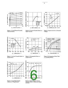
5. CURRENT TRANSFER RATIO in percent is defined as the ratio of output collector current, IO, to the forward LED input
current, IF, times 100.
6. Device considered a two terminal device: pins 1 and 3 shorted together, and pins 4, 5 and 6 shorted together.
7. In accordance with UL 1577, each optocoupler is proof tested by applying an insulation test voltage ≥ 4500 VRMS for 1 second
(leakage detection current limit, II-O ≤ 5 µA).
8. Common transient immunity in a Logic High level is the maximum tolerable (positive) dVCM/dt on the rising edge of the
common mode pulse, VCM, to assure that the output will remain in a Logic High state (i.e., VO > 2.0 V). Common mode
transient immunity in a Logic Low level is the maximum tolerable (negative) dVCM/dt on the falling edge of the common mode
pulse signal, VCM to assure that the output will remain in a Logic Low state (i.e., VO < 0.8 V).
9. The 1.9 kΩ load represents 1 TTL unit load of 1.6 mA and the 5.6 kΩ pull-up resistor.
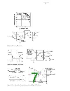
10. The frequency at which the ac output voltage is 3 dB below its mid-frequency value.
11. Use of a 0.1 µF bypass capacitor connected between pins 4 and 6 is recommended.

 AGILENT [ AGILENT TECHNOLOGIES, LTD. ]