Small Outline, 5 Lead, High
Speed Optocouplers
Technical Data
HCPL-M452
HCPL-M453
Description
Features
ThesesmalloutlinehighCMR,
highspeed,diode-transistoropto-
couplersaresinglechannel
devicesinafiveleadminiature
footprint.Theyareelectrically
equivalenttothefollowingAgilent
optocouplers:
• Surface Mountable
• Very Small, Low Profile
JEDEC Registered
Package Outline
• Compatible with Infrared
Vapor Phase Reflow and
Wave Soldering Processes
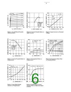
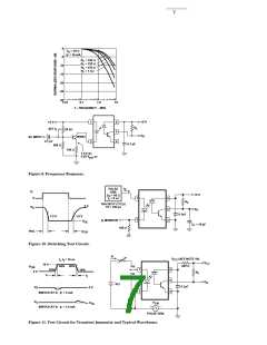
• Very High Common Mode
Transient Immunity:
15000 V/µs at VCM = 1500 V
Guaranteed (HCPL-M453)
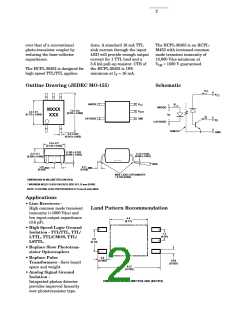
SO-5 Package
HCPL-M452
HCPL-M453
Standard DIP
SO-8 Package
HCPL-4502
HCPL-4503
HCPL-0452
HCPL-0453
• High Speed: 1 Mb/s
• TTL Compatible
(Note: These devices equivalent to 6N135/6N136 devices but without the base lead.)
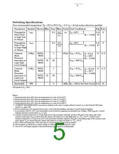
• Guaranteed AC and DC
Performance over
Temperature: 0°C to 70°C
The SO-5 JEDEC registered
(MO-155) package outline does
not require “through holes” in a
PCB. This package occupies
approximately one-fourth the
footprint area of the standard
dual-in-line package. The lead
profile is designed to be
These diode-transistor
optocouplers use an insulating
layer between the light emitting
diode and an integrated photon
detector to provide electrical
insulation between input and
output. Separate connections for
the photodiode bias and output
transistor collector increase the
speed up to a hundred times
• Open Collector Output
• Recognized Under the
Component Program of
U.L. (File No. E55361) for
Dielectric Withstand Proof
Test Voltage of 3750 Vac, 1
Minute
compatible with standard
surface mount processes.
• Lead Free Option
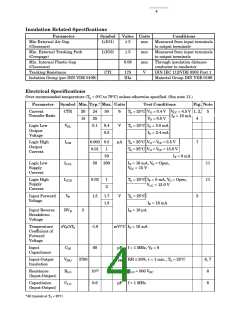
CAUTION: The small device geometries inherent to the design of this bipolar component increase the component's
susceptibility to damage from electrostatic discharge (ESD). It is advised that normal static precautions be taken
in handling and assembly of this component to prevent damage and/or degradation which may be induced by
ESD.

 AGILENT [ AGILENT TECHNOLOGIES, LTD. ]